
Roger Hill
Philips Research Laboratories
Surrey, England
A microstrip antenna array is one of the simplest forms of antennas available. The antenna consists of a single printed circuit board with an RF connector and perhaps an absorptive load. Microstrip antennas can be manufactured very inexpensively now that reasonably priced, closely controlled substrate materials are available. Microstrip antennas are very versatile and are suitable for applications requiring pencil beams, fan beams and omni-directional coverage. They offer a choice between linear polarization and circular polarization, and circuit components may be integrated with the antenna in many instances. Microstrip antennas can be flat or curved to suit the structure to which they are mounted. Now that microstrip antennas have come of age it is useful to review some of the lessons learned for their design.
This article is intended to serve as a practical guide to microstrip array design. Most of the work carried out by the author used experimental models, although the same qualitative understanding is required when using computer simulation techniques. No extensive theory is offered and important theoretical facts are simply stated as required. Where manipulation of data is required the methods are explained but no great detail is provided. The aim is to help the designer to make sensible decisions resulting in a successful product. This is explained in the text and, in some cases, backed with case examples.
THE RADIATING MECHANISM OF A MICROSTRIP TRANSMISSION LINE
An example of a microstrip transmission line is shown in Figure 1 and consists of a flat conducting strip suspended above a ground plane. The conducting strip is supported by a dielectric substrate and is normally manufactured by etching copper-clad material using photographic techniques. Microstrip provides an inexpensive and compact alternative to other forms of transmission line, and is used to make devices such as directional couplers, powers dividers and filters. These components are easily integrated with circuit modules such as amplifiers, attenuators and switches.

Microstrip circuits were originally confined to lower frequency applications (such as VHF or UHF) because of the apparently uncontrolled radiation, which took place at microwave frequencies. This characteristic was overcome when closely controlled high dielectric constant ceramic substrates became available and radiation was reduced to a tolerable level. Microstrip has now largely replaced other forms of transmission lines (such as triplate and waveguide) for the manufacture of microwave components and circuits. An exception is in high power applications.
The radiation, which occurs in microstrip circuits, is now better understood and is being exploited in the design of microstrip antennas. The key to understanding the radiation process is in the observation that straight lengths of microstrip line do not radiate. Measurements of test pieces using a low dielectric substrate several millimeters thick are found to have low transmission loss even at microwave frequencies. The performance is usually limited by the interface with a coaxial line, which may allow radiation. A good example where low radiation is essential is in the use of ultra-large, air-spaced microstrip lines to provide a controlled RF environment for the testing of electrically small antennas. An embodiment is shown in Figure 2 and is known as a form of TEM cell. The device under test is placed inside and comparative measurements of sensitivity are made. Radiation by the cell leads to fluctuations of the field inside as the operator moves around; however, this effect is prevented at frequencies up to the limit where high order modes propagate.

The reason radiation is prevented in straight microstrip line (and occurs in microstrip discontinuities) can be understood by looking at the electric fields shown in Figure 3. The fringing fields along the line are balanced causing the cancellation of any radiated energy. At the end of the line, where there is no balance of electric fields, the discontinuity radiates copiously. Radiation is more intense if wide transmission lines are used and this effect is associated with thick low dielectric constant substrates.

Several examples of microstrip discontinuity are given in Figure 4. In most cases electric fields are unbalanced and radiation occurs. An exception is example d, where the junction is perfectly balanced and radiation is prevented. The discontinuity can be represented by an admittance where radiation occurs and microstrip arrays can be made by "joining up" the admittances using straight microstrip lines. The characterisation of discontinuities and mutual coupling between radiators forms an important part of this tutorial.

MUTUAL COUPLING IN ANTENNA ARRAYS
Any account of antenna arrays must be preceded by describing the effects of mutual coupling between radiators. This is as true for microstrip arrays as for any other type of antenna array. To optimize and characterize an array element in isolation and to use the information to design an array antenna usually ends in disappointment.
So what does mutual coupling do? In particular it changes the radiation resistances of the coupled elements. This effect can lead to a poor match and often, depending on the feed mechanism, to a poor aperture illumination and poor sidelobes. To understand how this change of radiation resistance comes about requires examination of the example in Figure 5 where an array of slot elements is chosen for the purpose of illustration. The beam is very wide in the plane shown (the E-plane) and coupling is strong. The electric field contributions from each radiator can be combined as shown in the diagram. It should be noted that the vertical components of the electric field from each radiator at the midway positions are in opposition to the field of neighboring slots. Vertical electric field components cancel each other in these planes and the resulting field is horizontal. Vertical conducting plates can be placed in these positions either side of a slot without altering the fields of the radiator and other slots can be discarded. In other words, the vertical plates simulate the presence of other radiators. Now it is easy to see how mutual coupling changes the radiation resistance; the radiation is directed into a two-dimensional channel instead of all space.

Sideplates are commonly used to simulate mutual coupling in slotted waveguide arrays and absorbers are added at the ends of the plates to prevent reflections at the interface with free space. The radiator is then optimized and characterized under realistic conditions.
Another method of simulating mutual coupling for characterizing a radiator (and the most obvious) is to examine many elements at once. The elements are suitably spaced for the requirement and fed using the necessary phase slope. End elements have a different performance than central elements, but errors may be ignored provided sufficient elements are used.
Mutual coupling in array elements can also be examined using an antenna test range, as shown in Figure 6. The element to be investigated (which is matched in free space in this example) is tested initially in isolation on the test range. Similar elements are then added and terminated with loads. The measurement is repeated and compared with the performance of the isolated element. It can be seen that the signal is reduced depending on the angle of reception. This signal loss is manifested as a mismatch loss in a complete array and provides a powerful method of predicting (and hopefully avoiding) blind spots in phased arrays. The radiator matching mechanism is then adjusted for best results.

More descriptions of techniques used to simulate mutual coupling are given in the case examples to follow. First here are some of the most important points:
* Mutual coupling between radiators changes the match (or radiation resistance) of the radiator
* Mutual coupling does not change the amplitude and phase distribution significantly for corporate fed arrays (however, it will change the amplitude distribution in travelling wave antennas)
* The phase slope is an important factor in mutual coupling. The match is very dependent on the phase slope
* The difference in amplitude between adjacent radiators in an array is usually small and can be ignored
* Mutual coupling in the E-plane for dipole elements is small and is sometimes ignored. Similarly, mutual coupling for slot elements is small in the H-plane
* An element can not be characterised on reflection using passive elements to simulate mutual coupling conditions.
LINEAR MICROSTRIP ARRAYS
Linear arrays are used for fan-shaped coverage and can also form a building block for planar arrays. Some case examples are provided to illustrate the design procedure. The three main feed methods are shown in Figure 7.

First, the corporate feed, which is composed of a power divider with transmission lines to the individual radiators, is examined. Although this method is physically large and expensive, it is also the most broadband. Often the overall bandwidth is limited by the bandwidth of the radiators themselves. Corporate feeds are popular for phased arrays where phase shifters are inserted in the transmission lines to steer the beam direction electrically.
Next, the travelling wave feed is described. Radiators are coupled to a single transmission line and energy decays along the line length. To achieve a symmetrical radiated power distribution the radiator coupling factors are made asymmetrical. An absorptive load captures the remaining energy. It is important that the radiator spacing is not a multiple of half a guide wavelength so that reflections from the radiators have a different phase at the feed input and tend to cancel each other. As a result the beam is tilted from broadside in a travelling wave antenna. A good input match is generally obtained, but it helps, especially for short arrays using tight radiator coupling factors, to incorporate a matching section at each radiator. The bandwidth is often limited by the permitted beam pointing variation.
Finally, there is the resonant array. Here radiators are deliberately spaced a multiple of half a guide wavelength apart to produce a broadside pointing beam. Some radiator types can be represented by a shunt conductance and others are represented by a series resistance. For the former, the input voltage repeats at each radiator and the input conductance is equal to the sum of the individual radiation conductances (usually made equal to the characteristic admittance of the microstrip line for a good match). In the case of series radiators the current repeats at each radiator and the input resistance is equal to the sum of the individual radiation resistances. No absorptive load is used in either case and the radiator coupling factors are symmetrical for a symmetrical power distribution at the aperture. The match usually limits the bandwidth.
Now that the principles of mutual coupling in arrays and linear array feeds have been described, two design case examples are presented. The purpose is to demonstrate how this knowledge may be applied in practice.
CASE EXAMPLE 1
In this first example the configuration described by James and Wilson1 is used to make a linear travelling wave array to meet the following performance:
H-plane beamwidth: 10°
H-plane beam pointing: 30° towards feed
H-plane sidelobe level: 22 dB max
This linear array was used as a building block for a planar array described by Gibson and Hill,2 and the design proceeded as follows:
The James and Wilson microstrip array configuration is shown in Figure 8a and consists of a central feed with stubs attached. The stubs are nominally a half wavelength long in the medium and the radiating fields seen at either end are in phase. The stub spacing is also in the region of a half wavelength and the actual value determines the beam pointing angle. Data of the stub radiation conductance for different stub widths is required to design the antenna.

A number of test pieces, each using stubs of equal width, were made to obtain the data. The stub spacing was chosen to achieve the required squint angle to simulate realistic mutual coupling conditions. A microstrip line of similar length but without stubs was also made. The radiation conductance was then determined from the loss difference of the test pieces with and without the stubs. The data was then used in computations of stub width to achieve the aperture distribution with maximum radiation efficiency. Matching sections were also added as shown in Figure 8b to reduce standing waves along the feed line and to improve the side lobe performance.
The differential through phase of test pieces with and without stubs was also examined, and the performance is shown in Figure 8c. This information was used to determine the precise stub length so that the operation was near the point of inflection.
The maximum sidelobe level of the complete array was 21 dB close to the design value. The radiation efficiency was 74 percentage in accordance with design predictions.
CASE EXAMPLE 2
The design of an omni-directional travelling wave microstrip array3 is described in another case example. The antenna uses a single printed panel, as shown in Figure 9a, and consists of a series of microstrip transmission lines where the ground planes are of varying width and alternate on either side of the board. Radiation occurs at the crossover points of the microstrip ground planes and the amount of radiation is controlled by the ground plane width. It is found that good omni-directional performance is maintained provided the ground plane width is limited to approximately a quarter wavelength.

Data of radiation conductance as a function of ground plane width were required for the design of arrays and were obtained, as for case 1, by using several arrays consisting of radiators of constant size. Again the elevation beam pointing angle was set to be consistent with the requirement for realistic mutual coupling conditions. The radiation conductance values were then deduced from the through loss measurements of the arrays and a graph of radiation conductance versus radiator width was produced.
Initial array designs were unsatisfactory and it was found that there was a large shunt capacitance at each radiator. This caused a severe standing wave along the array which upset the aperture distribution. It helped substantially to stagger the ground planes ends on either side of the board from each other, as shown in Figure9b, which reduces the capacitance. The complete solution was to design matching sections to neutralize reflections from both the capacitance and conductance at each radiator. An alternative method is to use small stubs with plated holes at each radiator, as shown in Figure 9c. The stub dimensions are chosen to neutralize the junction capacitance and this method may be of special use in resonant arrays.
The performance of an antenna design is shown as an example in Figure 9d. The antenna was constructed using 1/16" material with a dielectric constant of 2.1. The travelling wave design operated at 4.8 GHz and provided an upward pointing beam. The overall length was 34 cm. and the peak gain was 9.8 dB with respect to an isotropic radiator. The estimated radiation efficiency was 83 percent.
PLANAR MICROSTRIP ARRAYS
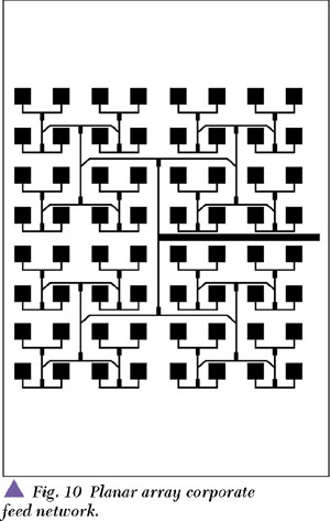
Planar microstrip arrays are used to form a pencil beam and array elements can be fed in a variety of ways. In the first example the corporate feed is used to activate every array element separately. An example is shown in Figure10,4 which consists of patch radiators and a network of microstrip feed lines. The patch feeds are inset to achieve a good match to the feed lines. The feed lines are made of similar length so the beam pointing is broadside to the array at all frequencies. The bandwidth is limited by the patches themselves, which is typically a few percent. Feed lines are rather long, adding to loss mechanisms, and spurious radiation is caused at bends and junctions.
The next example involves several linear arrays fed using a corporate feed. An example is shown in Figure 11, which uses the previously described linear travelling wave arrays. The corporate feed is compact but rather lossy, and the overall radiation efficiency was estimated at 40 percent.2 The residual energy of each linear array is combined into a single load using a second corporate feed network.

A planar resonant feed5 may be used consisting of a lattice of hexagons, squares or equilateral triangles, and an example of a hexagonal array is shown in Figure 12. The line lengths are one-half wavelength in the medium and a voltage introduced at the feed is repeated at each line intersection. Radiation may be induced in a variety of ways and horizontal lines are made wider in the case shown. This causes the necessary asymmetry for radiation at the junctions and all radiation has the same phase producing a broadside beam. The line width is adjusted experimentally to provide the required input impedance (50 Ω). The antenna is very compact and the whole area forms part of the radiating structure. The radiation efficiency is relatively high (62 percent in the example); however, the antenna is only suitable for narrow band applications.

It is possible that the performance may be further improved by preventing spurious radiation at the array boundary. This can be accomplished using quarter wavelength stubs with a short circuit to ground, as shown in Figure 13. The short circuit conveniently takes the form of a plated hole and the arrangement should result in reduced sidelobes and increased radiation efficiency.

SUMMARY AND FUTURE TRENDS
The advantages of microstrip antenna arrays, namely low cost, compactness, simplicity and versatility, are now well appreciated. It is hoped that this article has highlighted some of the practical considerations required for successful designs.
The performance of linear arrays is of a high order and radiation efficiency up to 75 percent can be obtained. Side lobe levels of 25 dB are often achieved. Although the performance of microstrip planar arrays is sufficient for many applications, better radiation efficiency is often desirable. Certainly microstrip cannot compete with waveguide arrays for efficiency. Perhaps some future needs can be satisfied using a combination of waveguide and microstrip to achieve middle-of-the-road performance and cost. A possible embodiment of this approach is shown in Figure 14.

Several linear microstrip arrays are printed on a single board and are fed using a linear waveguide. The waveguide is formed from a metal channel, which is joined to the ground plane on the back of the microstrip board. Coupling between waveguide and microstrip is achieved using slots etched in the ground plane of the printed panel. The coupling factors are determined by the displacement of the slots from the waveguide centerline.
The construction is much less expensive than for a waveguide array and the radiation efficiency promises to be better than a microstrip array. The better sidelobe capability of waveguide arrays is retained in the horizontal plane in the example shown. *
References
1. J.R. James and G.J. Wilson, "New Design Techniques for Microstrip Antenna Arrays," Proceedings of the 5th European Microwave Conference, September 1975, p. 102.
2. P.J. Gibson and R. Hill, "A Planar Microstrip Array," IEE Colloquium Advances in Printed Antenna Design and Manufacture Digest, No. 1982/19, pp. 3/13/3.
3. R. Hill, "A Twin Line Omni-directional Aerial Configuration," Proceedings of the 8th European Microwave Conference, September 1978, pp. 307311.
4. L. Leyton and G. Dolmans, "Smart Antennas for High Bit-rate Indoor Communication," Millennium Conference on Antennas and Propagation, Davos, Switzerland, April 914, 2000.
5. R. Hill, "Printed Planar Resonant Arrays," 5th International Conference on Antennas and Propagation, York, 1987, pp. 473476
 Roger Hill studied physics at University College London, where he graduated in 1967. Since then he has designed a wide range of antenna systems and RF components for several companies, chiefly Racal and Philips. These designs have been based on waveguide and triplate but most of all microstrip transmission line. Antennas have always been of deep interest, and, in particular, understanding the underlying principles of operation for successful design. As a result, some of the practical aspects of microstrip array design have been grouped together in this article based on his experience. Hill has authored several papers, including printed antenna design, and is presently working at Philips Research Laboratories on antennas for mobile telephone handsets.