
The GaAs HEMT and PHEMT
The acronym "HEMT" stands for: High Electron Mobility Transistor. In a HEMT the channel is effectively a quantum well. And a quantum well is a depletion region within an undoped GaAs layer that has been created by a heterogenous junction made using highly doped GaAs-based semiconductor materials. For example this heterogenous junction could be P-N where both the P and N regions are highly conductive. The channel is referred to as a two-dimensional electron gas (referred to as “2-DEG”) in the channel beneath the gate and it has a very high conductivity. These effects can be greatly enhanced by ensuring the doped and intrinsic layers possess slight crystal lattice mismatches. This situation is defined as “pseudomorphic” and it gives rise to the term “PHEMT”, hence a GaAs pseudomorphic HEMT or GaAs PHEMT. These properties lead to very high frequency operation–well into the mmWave bands.
The GaN HEMT
The wide bandgap semiconductor know as gallium nitride (GaN) is a truly revolutionary compound material–particularly notable for its application in RF electronics technology. Transistors based upon GaN, specifically the GaN HEMT provide exceptional characteristics for power and also low-noise applications. A cross-section of such a transistor is shown in Figure 2.
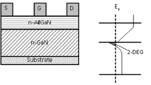
Figure 2 Cross-sectional structure and energy-level diagram for a GaN HEMT.1
GaN HEMTs are manufactured either on silicon or on silicon carbide (SiC) substrates. SiC provides an excellent heat sink which is important for power devices.
It is also possible to replace the n-GaN layer by n-AℓN (aluminium nitride) but this will not be elaborated upon further here.
GaN HEMT transistors tend to demand relatively high-voltage supplies, such as 40 V or more. They are mainly oriented toward medium-to-high power requirements and–as discrete devices with efficient heat sinks–can deliver in the order of many hundreds of Watts continuous-wave (CW) at relatively low microwave frequencies such as L- or S-Band.
Many GaN HEMTs are designed for use well into mmWave–particularly small-signal devices. And most of these types of transistors form the major “process” in MMICs of various types. GaN HEMT developments in relation to distributed amplifiers are considered in detail by Ghavidel et al.2 GaN technology is now becoming common across almost all RF applications. In particular active electronically-scanned array (AESA) radar modules increasingly adopt GaN technology.
MMICs and RFICs
Fully integrated microwave (or RF) ICs are widely available and the semiconductor processes are CMOS, SiGe BiCMOS, GaAs PHEMT or GaN HEMT.
The following commonly-encountered terms are essentially interchangeable;
- Monolithic microwave integrated circuit (MMIC), or;
- Radio-frequency integrated circuit (RFIC).
There are some arguments regarding the strict applicability of each terminology but the outcome is largely academic and will not be followed-up here. The MMIC abbreviation conveniently pronounces “M(i)MIC.”
Unlike integrated circuits designed for digital subsystems (ICs or "chips"), those designed for RF or microwave applications cannot merely comprise the transistors–interconnected by conductor arrays. Instead a combination of semiconductor devices (diodes and transistors) and passive circuit elements is required. The final MMIC may embody a specific microwave circuit function such an amplifier or a mixer–or it may comprise a much more comprehensive subsystem.
In most instances (although not exclusively) the more comprehensive MMICs tend to be those realized using either RF CMOS or SiGe BiCMOS technologies. The economic case is particularly strong where high-volume manufacture is the case. Major manufacturers of these more comprehensive chips offer fully integrated subsystems that include several ADCs, several DACs–and many further “sub-circuits” all on the same chip.
Specific MMIC design approaches require the initial choice as to the transistor technology that will be implemented. This is always referred to as the “process.” It means that a specific manufacturer (a “foundry”) will for example operate a publicized GaAs PHEMT “process” or a GaN HEMT “process”–for example.
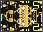
Figure 3 10 W MMIC Chip (with acknowledgement to Paul Khanna and Transcom Inc. for permission to reproduce this image).
A photograph (see Figure 3) in article by Paul Khanna3 is a MMIC chip capable of 10 W of output microwave power (Transcom Inc. as well as Paul Khanna are thanked for their permission to reproduce this image). As well as diodes and transistors, air-bridges, capacitors, inductors, resistors and Lange couplers are all regularly realizable on-chip.
Densely-packed mixed-signal RFICs enable combinations of analog (RF) and digital circuitry to be created on the same chip. Thus ADCs and DACs, for example, are simultaneously processed on-chip. In particular time-interleaved ADCs (particularly important in microwave systems) can be co-processed.
Providers of EDA software, such as Ansys, Keysight Technologies or NI AWR, offer well-established and regularly updated design software that handles MMIC design as well as hybrid RF circuit design suites.