
An accurate and compact large-signal model is proposed for modeling heterojunction bipolar transistors (HBT) fabricated on InP material. In DC mode, the model includes self-heating and soft-knee effects, as well as the temperature dependence of the model parameters. In small-signal mode, the model captures the variation of various AC parameters with bias. The procedure of extracting the model parameters uses DC and multiple bias S-parameter measurements. The validity and the accuracy of the large-signal model are assessed by comparing the simulation with measured DC characteristics, small-signal behavior and large-signal operation of an InP HBT.
The HBT is an attractive device for microwave and mmWave amplifier applications because of its high-power density. This is due to its vertical structure, which enables a large current handling capability.1-2 For designers, it is important to use a reliable large-signal model, developed from the measurements under various bias conditions of the device, for an accurate prediction of circuit performance parameters, such as gain and distortion. This requires an accurate DC model, on the one hand, and a precise description of the variation of the small-signal intrinsic elements with bias and frequency, on the other. A number of articles have described the large-signal models of HBTs in an effort to create models that are valid over a wide range of operating biases and frequencies.3-5 The basic physics of HBT operation can be described by back-to-back diodes and controlled current sources, as found in the Ebers-Moll (EM) and Gummel-Poon (GP) models. Following the same basic philosophy, a number of full-featured models are now available, such as the Agilent, Ferdinand-Braun-Institut fur Hochstfrequenztechnik (FBH) and University of California, San Diego models for III-V compound HBTs. Although these models are mature and allow for reliable simulations of nonlinear circuits, there are, and always will be, some challenges, such as operation under high-power conditions with distributed effects.6
The purpose of this article is to set up a self-built, flexible, nonlinear, large-signal InP HBT model implemented as a symbolically defined device (SDD) in a Keysight ADS simulator. The large-signal model includes most characteristics of InP HBTs. The self-heating effect is expressed by a resistor-capacitor (RC) thermal sub-circuit. The soft-knee effect, which results from the potential spike in InP HBTs, is modeled with a bias-dependent collector resistance. With improving technology, new effects occurring in the device can be conveniently added to the SDD model. The validity and the accuracy of the large-signal model are assessed by comparing the simulation with measurements of DC characteristics, small-signal behavior and large-signal operation for a 1 x 10 μm2 InP HBT.
HBT MODEL
The final model topology is shown in Figure 1. At first glance, it resembles most HBT models, but the specifics of each component have been adapted to this transistor. Some elements have been borrowed from various studies and models by other researchers. The charge model is the same as that adopted by Rudolph and Doerner.7 The base-collector, base-emitter and collector-emitter current formulations are based on classical temperature-dependent diode relationships. Self-heating is calculated using a simple, one-pole RC network, as is commonly used in nonlinear models such as Mextram, vertical bipolar inter-company (VBIC) and high current model (HICUM).
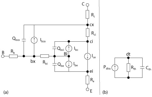
Figure 1 Large-signal equivalent circuit (a) and thermal (b) models of an InP HBT.
DC Characteristics
The DC equations are based on the VBIC model. The base-emitter and base-collector currents cover the ideal and non-ideal (recombination) behavior.
Two parallel diode currents are used: one for the “ideal” part (index I), the other for the “non-ideal” part (index N) of the base-collector or base-emitter current. The variable x in the formula is used to denote either base-collector (c) or base-emitter (e). IBXN and IBXI are the non-ideal and ideal saturation currents, respectively. nXN and nXI are the non-ideal and ideal current ideality factors, respectively. Vbxi is the junction voltage, and vt is the temperature voltage. The diode current, Ibcx, is the extrinsic part of the base-collector current.
The collector current source Ice is determined by the two transport current terms Icf and Icr:
where Is and nf are the forward collector saturation current and ideality factor, respectively. Isr and nr are the reverse emitter saturation current and ideality factor, respectively.
For the DC characteristic, one of the most important physical effects of InP HBTs is the soft-knee effect. A physical reason for this phenomenon is that for high-level injection, the corresponding injected electron density increases, compensating for the collector doping concentration. When the electric field at the base-collector junction is sufficiently reduced, electron transport ceases to be primarily drift current. Meanwhile, the rising of the energy band at high current densities can block electron transport by band energy discontinuity. The effect is equivalent to an increase in collector resistance. The voltage drop in the collector resistance causes a reduction in the electric field at the base-collector junction. The resistor is modeled with a bias-dependent collector resistor Rci in this work:
where a, b and I0 are the fitting parameters.
Small-Signal Behavior
The charge model adopted is the same as that used in the FBH model, which itself is based on the Mextram formulation. Charge-based models tend to have better convergence properties and avoid nonphysical results, which may occur when using capacitance expressions. The depletion charge is given by:
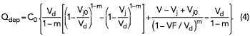
where the voltage is limited to eliminate a pole in the charge function. Here, Vjo and Vd are the limited junction voltage and diffusion voltage, respectively, while C0 is the junction capacitance at zero volts. There is also VF, a transition parameter related to the pole-elimination mentioned earlier. The junction grading coefficient, m, is typically between 0.3 and 0.5.