
A Wideband, Varactor-tuned Microstrip VCO
Matjaz Vidmar
University of Ljubljana
Slovenia
When electrical tuning of an oscillator is required over a wide microwave frequency range, yttrium iron garnet (YIG)-tuned oscillators usually provide the widest frequency coverage as well as relatively low phase noise. While YIG-tuned oscillators generally provide a tuning range of more than one octave, the tuning range of varactor-tuned VCOs is much more restricted. Furthermore, all available varactors are rather lossy capacitors with low Q values at frequencies above 1 GHz, degrading the phase noise of the oscillator.
Wideband, varactor-tuned microwave VCOs are usually built as hybrid microcircuits to reduce device parasitics. Expensive GaAs varactor chips are used to simultaneously increase the frequency coverage and reduce the phase noise due to the better Q of GaAs varactors when compared to their silicon counterparts. Although varactor-tuned VCOs cannot compete with YIG VCOs directly, significant improvements can be made with a better varactor-tuned VCO circuit design.
This article presents the design of a varactor-tuned VCO covering an octave frequency range up to 4 GHz and more. The VCO design uses standard surface-mount device (SMD) components, including inexpensive silicon varactors. Furthermore, the VCO is built using conventional microstrip technology on inexpensive FR-4 circuit-board laminate. Finally, the phase noise of the described VCO is reasonably low (approximately 20 dB worse than a free-running YIG oscillator).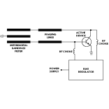
Wideband VCO Design
Wideband VCO design with negative-resistance active devices is difficult due to circuit parasitics. Two-port amplifier devices offer the designer more freedom. A basic microstrip oscillator design with a two-port amplifying device is shown in Figure 1 .
Any oscillator design requires an amplifier and a frequency-selective feedback network. Besides the desired frequency response, the feedback network should also provide the correct phase shift so that the total phase shift in the feedback loop equals an integer multiple of 360°. Of course, this total phase shift also includes the phase shift inside the active device, which is usually much larger than 180° due to device and package parasitics at microwave frequencies.
In the case of a microstrip oscillator, the feedback network may include an interdigital bandpass filter to determine the oscillator frequency. Additional phasing microstrip lines are required to bring the total phase shift to an integer multiple of 360° at the desired operating frequency. In addition, the feedback network should be designed so that oscillation is only possible at the fundamental mode of the interdigital bandpass filter, while oscillations at higher order resonance are suppressed.
A fixed-frequency oscillator can be modified into a VCO by inserting one or more varactors into the circuit. If a single varactor is inserted in series with the central finger of the interdigital bandpass, frequency coverage of approximately 10 percent around a central frequency of 2 GHz can be obtained. Although a single varactor may tune the interdigital bandpass over a wider frequency band, the desired phase shift cannot be maintained over the wider range to keep the oscillator running.
A wideband microstrip VCO can be built only if the phase velocities of all microstrip lines are controlled. The phase velocity of a microstrip line can be controlled using several series or parallel variable reactances distributed along the microstrip line. A series connection is usually used at microwave frequencies due to the relatively high capacitance of available varactors.
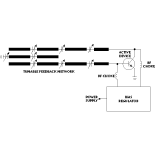 A tunable microstrip oscillator design is shown in Figure 2 . The phase velocity of the microstrip lines is controlled by several variable capacitors connected in series in the transmission lines. The capacitors adjust both the center frequency of the microstrip bandpass filter and the overall phase shift of the feedback network. If the spacing between adjacent variable reactances is kept sufficiently small (less than one-quarter wavelength at the maximum operating frequency), very wide tuning ranges are possible.
A Practical S-band VCO
The circuit diagram of a practical wideband, varactor-tuned microstrip VCO operating in the S-band (2 to 4 GHz) is shown in Figure 3 . The feedback network includes an interdigital bandpass filter tuned with six type BB833 silicon, hyperabrupt varactors (0.75 pF minimum capacitance, 1.8 W series resistance, SOD-323 SMD package). Several 22 kW resistors are used as resonance-free RF chokes to apply the same tuning voltage to all six varactors.
Due to the low Q of the varactors used, the insertion loss of the feedback network is rather high. Therefore, a type BFP420 high ft silicon bipolar transistor (ft = 25 GHz, SOT-343 SMD package) is required as the active device. The DC bias is provided by a simple resistor network. In order to isolate the oscillator, only a very small fraction of the RF signal is taken through a resistive divider from the collector to the output.
 Some components are required only to simplify the printed-circuit-board layout (for example, the series connection of two 4.7 kW resistors for the base bias). Other components are required to suppress unwanted resonances, such as the two 100 W resistors in the varactor bias circuit. Finally, the VCO is followed by two buffer stages to further isolate the output, as shown in Figure 4 .
The microstrip circuit was etched on 0.8-mm-thick, double-sided FR-4 glass fiber-epoxy laminate. Two different layouts were tested, both with dimensions of 20 mm x 80 mm, as shown in Figure 5 . The narrowband version uses higher impedance microstrip lines in the feedback network, resulting in stronger coupling and lower insertion loss. The wideband version uses wider microstrip lines, resulting in weaker coupling and higher insertion loss, but with wider frequency coverage using the same varactors. All passive SMD components (resistors and capacitors) are standard size 0805 parts.
If the described VCO is to be redesigned for different frequencies and/or different varactors, the circuit size first should be scaled. Second, the center finger of the microstrip bandpass should be tuned to obtain the correct phase shift in the feedback loop. If tuning of the center finger shifts the operating frequency range too much, the entire circuit must be scaled again. Next, tracking of the amplitude and phase response should be checked while adjusting the varactor tuning voltage. Finally, the amplitude response should be checked both at the desired frequency and at the undesired higher order resonances of the microstrip feedback network. This design procedure applies equally to computer simulation and practical circuit tests.
The VCO's Measured Performance
Three versions of the described VCO were built. The first version was built on the narrowband PCB 1 with BB833 varactors. The second version was built on the wideband PCB 2 (also with BB833 varactors). The third version was built on PCB 1 with better BB857 silicon hyperabrupt varactors (very small SCD-80 SMD package, 0.55 pF minimum capacitance and 1.5 W series resistance). Several samples of all three versions were built and tested.
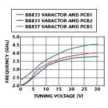 The typical tuning curves of all three VCO versions are plotted in Figure 6 . The first version covers 2 to 3.85 GHz, depending on the tolerances of the varactors used. The tuning range of the second version is approximately 150 MHz wider, covering 2.05 to 4.05 GHz with the same varactors. The tuning range of the third version extends from 2.4 to 4.6 GHz thanks to the improved BB857 varactors.
The tuning range of all three versions can be extended by approximately 50 MHz on the lower end by allowing the tuning voltage to turn negative to -0.7 V. The tuning curves are quite nonlinear. The tuning slope exceeds 100 MHz/V at tuning voltages of approximately 7 V and falls below 10 MHz/V at tuning voltages of approximately 30 V. Since the VCOs were designed for the widest frequency coverage, no attempt was made to linearize the frequency/voltage response in the RF circuit.
Since specialized phase noise test equipment was not available, the phase noise of the available model HP8593EM spectrum analyzer was first roughly estimated. The phase noise of the analyzer was determined to be sufficiently low to accurately measure the phase noise of the described VCOs. Two samples of the first and second versions (with BB833 varactors) were packaged in shielded cases and connected to well-filtered supply and tuning voltage sources.
The single-sideband (SSB) phase plots, shown in Figure 7 , demonstrate that the described VCOs are roughly 20 dB worse than the YIG oscillator inside the spectrum analyzer. Interestingly, the phase noise is approximately 5 dB stronger at the band center than at the band edges, suggesting that at least part of the phase noise is caused by thermal noise voltage generated in the 22 kW resistors that is modulating the VCO frequency at the point where the tuning slope is the steepest.
Possible VCO Improvements
Although the frequency coverage of the described VCO exceeds the advertised performance of commercially available hybrid VCOs, many improvements to the described circuit are still possible. In particular, the phase noise performance probably could be improved. Last, but not least, the described VCO design can be readily adapted to other two-port active devices, such as GaAs FETs, high electron mobility transistors, heterojunction bipolar transistors or MMIC amplifiers.
Part of the phase noise is caused by the 22 kW resistors used as resonance-free chokes to bring the tuning voltage to the varactors. Lower resistor values cannot be used since the RF circuit losses increase. True RF chokes (inductors) should be selected carefully to avoid parasitic resonances in the frequency range of interest.
The phase noise performance could also be improved by replacing the simple resistor bias network of the BFP420 transistor. Since the S parameters of bipolar transistors depend mainly on the DC bias currents through the transistor, the transistor's operating point should be accurately stabilized to further improve the phase noise performance.
Both the phase noise and long-term (thermal) stability of the VCO could be improved by using a better microstrip material than the suggested FR-4 glass fiber-epoxy laminate. This material has a high temperature coefficient, shifting the VCO frequency downwards by a few megahertz for each degree of temperature increase. Besides lower temperature coefficients, suitable microwave substrates should also provide lower losses and higher Qs for the microstrip resonators.
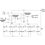 The nonlinear frequency/voltage response of the described VCO design may require a linearizer. A simple tuning slope linearizer circuit is shown in Figure 8 . The gain of the two operational amplifiers is set to the lowest value around the reference voltage of +7 V DC (where the VCO tuning slope is the steepest). At lower and higher tuning voltages, some positive feedback is switched in so that the overall gain increases to compensate for the decay that occurs in the tuning sensitivity.
The requirements for the linearizer response could also be estimated form the varactor diode capacitance (CT = f(VR)) curves shown in Figure 9 . Curves for the BB833 and BB857 varactors clearly show that the maximum relative capacitance change occurs between 5 and 10 V. Above 15 V, the capacitance curves become flat, resulting in a decrease in the VCO's tuning slope.
The presettable potentiometers P1 to P8 permit the switching points to be set. Since the upper part of the tuning curve is much more nonlinear than the lower part, six switching points are used in the upper part (resistors R+) and only two switching points are used in the lower part (resistors R-). Besides using low noise operational amplifiers, the resistor values should be selected carefully to avoid excessive noise generation in the linearizer circuit (resistor values too high) or excessive power dissipation (resistor values too low).
Conclusion
A varactor-tuned VCO has been designed that uses standard SMD components and inexpensive silicon varactors. The VCO's frequency tuning range is over one octave and extends above 4 GHz. The VCO is built using low cost FR-4 PCB material and achieves good SSB phase noise performance.
Acknowledgment
The author wishes to thank Knut Brenndoerfer of Siemens Semiconductors, Munich, Germany, for supplying the many different varactors and other SMD semiconductor samples without which the described VCO could not have been developed.
Matjaz Vidmar received his BSEE and MSEE from the University of Ljubljana, Slovenia in 1980 and 1983, respectively. He received his PhD in 1992, also from the University of Ljubljana, for developing a single-frequency GPS ionospheric correction receiver. Vidmar is currently teaching undergraduate and postgraduate courses in electrical engineering at the University of Ljubljana. His current research includes high speed electronics for optical fiber communications. Vidmar is also taking part in amateur satellite projects. He developed very high efficiency VHF and UHF transmitters that were successfully flown in space on the Microsat mission in 1990.