
Miniaturized Low Cost 30 GHz Monolithic Balanced BPSK and Vector Modulators: Part II
Part one of this two-article series analyzed single-stage and balanced topologies in detail. It was illustrated that a common technique for realizing direct biphase-shift keying (BPSK) microwave modulators is to employ reflection-type topology with cold pseudomorphic high electron mobility transistors (pHEMT) acting as variable resistance elements connected to the coupled and direct ports of a Lange coupler. However, at higher frequencies the parasitics of the cold pHEMTs start to dominate, resulting in large amplitude and phase error characteristics. It was determined that these parasitics can be removed by employing the balanced topology, which provides near-perfect amplitude and phase balance even at mm-wave frequencies. However, it was also noted that the balanced topology would, in theory, require twice the chip space of the single-stage topology. A novel microstrip coupler has been proposed that can be employed in the modulator designs to reduce the size of the MMIC circuits. This second article examines the physical realization of the compact microstrip coupler and its measured performance. The design and performance of the MMIC balanced biphase amplitude and vector modulator that employ the designed miniaturized coupler then are presented.
A.E. Ashtiani, T. Gokdemir, G. Passiopoulos and A.A. Rezazadeh
King's College London, Department of Electronic Engineering, Microwave Circuits and Devices Group, London, UK
S. Nam and I.D. Robertson
University of Surrey, Department of Electronic Engineering, Microwave and Systems Research Group Guildford, Surrey, UK
The balanced modulator topology requires a total of four couplers, one each for the input and output and one within each single-stage branch. Generally, in monolithic designs, a 3 dB power split is achieved by employing Lange couplers. However, Lange couplers (folded) require a total of five fingers and the overall length of the coupler is determined by the quarter-wavelength-long coupled fingers.1 For an MMIC chip it is essential to minimize the expensive chip area to reduce the cost, and Lange couplers in particular tend to use most of the area due to the quarter-wavelength sections. Thus, for a balanced modulator that requires a total of four Lange couplers, the coupler layout must be made as compact as possible and have the ability to be meandered to minimize the layout area.
A microstrip transmission line has an inhomogeneous dielectric, that is, the dielectric is part dielectric substrate and part air. It is important to note that microstrip parallel-line couplers have an odd- and even-mode property, which always results in Zoe and Zoo. Hence, the unequal odd and even modes excited in the coupled region exhibit different phase velocities and, consequently, different wavelengths. This inequality shows itself in the coupler's poor directivity. The other disadvantage of a parallel-coupled microstrip coupler is that a 3 dB power split cannot be obtained because it requires the two transmission lines to be very close to each other - on the order of 1 mm or less. However, such small separation is not possible due to fabrication limitations.
To avoid these problems, a number of publications2,3 have demonstrated that it is possible to equalize the different phase velocities over quite a broad band and achieve 3 dB coupling by introducing capacitors at the edges of the coupled region between the two lines. The new proposed multilayer directional coupler consists of two parallel-coupled microstrip transmission lines (compared to five fingers) and provides a 3 dB power split with a coupled length that is shorter than the standard quarter-wavelength.
The two parallel-coupled microstrip transmission lines are separated by 5 mm. Simulations using the Sonnet em® software package were performed on 95-mm-long subsections and included the various dielectric layers. This detail was necessary to account for the multiple dielectrics used in the foundry process. The simulated sections were then cascaded on HP EEsof Series 4 software with polyimide metal-insulator-metal (MIM) capacitors and included the remainder of the 50 W feed lines and RF on-wafer probe pads to obtain the overall response. The overall circuit is then optimized for the center frequency of 30 GHz. The top metal layer M3 and bottom layer M2 are used to form the plates of the capacitor and are separated with 1.4-mm-thick polyimide.
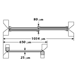 Figure 1 shows a comparison between the two layouts of a standard Lange coupler and the new miniature coupler at 30 GHz center frequency. It can be seen that the overall length of the miniature coupler is almost half and the width is less than a third of the standard Lange coupler.
The coupler fabrication was performed at GEC Marconi using its F40 foundry process. A microphotograph of the chip is shown in Figure 2 . The chip measures 0.85 mm x 1.10 mm including the 50 W feed lines and RF on-wafer probe pads. The coupler itself has a coupled length of 470 mm excluding the feed lines and has the potential for meandering to obtain an even more compact layout. The two-coupled transmission lines measure 10 mm wide and have even- and odd-mode impedances of 139 and 26 W, respectively. The GaAs substrate is 100 mm thick and has a dielectric constant of 12.8. The resulting even- and odd-mode effective dielectric constants (eeff) for the coupler are 5.1 and 4.05, respectively, and the calculated ratio of guided wavelength (leven/lodd) is 0.891.
Detailed simulations have shown that the effect of the MIM capacitor is to increase coupling and move the coupler's center frequency lower if the coupled length is kept constant. In other words, the capacitor effectively shortens the  length of the coupled region at the required center frequency. The simulated and measured performances of the miniaturized coupler are shown in Figure 3 . It can be seen that the device is well matched with good amplitude and phase responses. The simulated results are in good agreement with measured results. However, the measured input match differs slightly from simulated results. The main goal was to reduce the aspect ratio; this reduction may be achieved by reducing the widths to very small values. However, the resulting coupler is sensitive to process variations. Therefore, a small deviation from the actual width can lead to a large change in input matching.
The Balanced Modulator's Design and Measured Performance
The cold pHEMTs were incorporated in the simulation using S parameters measured on a test wafer. The other main component, the microstrip coupler, was modeled with Sonnet em and optimized to be incorporated into the overall circuit. Finally, all the remaining circuit elements such as thin-film resistors, capacitors, microstrip lines and RF on-wafer probe pads were modeled using foundry smart library models.
The microphotograph of the biphase amplitude modulator chip designed for operation at 30 GHz (which measures 1.1 mm x 0.9 mm) is shown in Figure 4 . The frequency response and static constellation were measured using a Cascade on-wafer probe station and model HP8510B vector network analyzer.
 Figure 5 shows the measured constellation of the balanced biphase amplitude modulator at 30 GHz for bias points between +1 and -2 V. The results proved that the cold pHEMTs act like 50 W resistors and provide maximum attenuation at the -0.55 V bias point. This result is in good agreement with the earlier theoretical analysis, which predicted the same bias point.
Figure 6 shows the simulated and measured frequency performance of the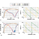 balanced biphase amplitude modulator at 30 GHz. The circuit achieved good impedance matching with minimal amplitude and phase errors over the 20 to 32 GHz frequency range. A phase difference of 180° between the on and off states was also maintained across a wide bandwidth. It can be seen that the measured results are in good agreement with the simulated results. The estimated insertion loss was only approximately 1 dB higher than the actual measured value.
The cold pHEMTs are controlled with an analog gate-source voltage signal Vgs, which was necessary to provide a continuous range of both positive and negative 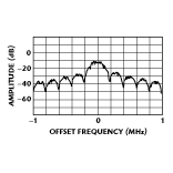 transmission coefficient amplitude values. For the practical demonstration, a PC with a digital-to-analog converter (DAC) card was used to generate a pseudorandom sequence and then generate the analog control voltages. As an example of measurement, Figure 7 shows the output spectrum of the BPSK signal at 30 GHz measured on a model HP8562 spectrum analyzer. The maximum bit rate that can be applied to the cold pHEMTs is set by the RC time constant on the gates. This time constant is minimized by using the smallest FET device geometry and by setting the gate bias resistor to the lowest value without degrading isolation. The chosen FET geometry is 2 ¥ 60 mm and the gate biasing is through a 600 W resistor. The measured results can be fine-tuned by controlling the DC bias level with a computer to obtain a better response and correct any degradation in performance due to fabrication process variations. The cold pHEMTs are operated at zero drain bias and the complementary signals on the gates are used to change switch states. Thus, the power consumption is very low and the maximum power handling limit of the circuit is set by the widths of the transmission lines used rather than the cold pHEMTS.
The Balanced Vector Modulator
Two generic types of microwave vector modulators are available. The first type consists of an attenuator in cascade with a 360° phase shifter.4 The second type is a tandem modulator consisting of two orthogonal channels that are individually amplitude modulated and then power combined in phase. The tandem modulator is commonly referred to as the in-phase/quadrature phase (I/Q) vector modulator, and a 3 dB coupler is used to create the two quadrature channels. Each channel is a biphase amplitude modulator like the one described in this article, and the output signals from these two biphase amplitude modulators are then combined in phase with a 3 dB Wilkinson power combiner.
When dealing with quadrature modulation schemes, it is useful to think of an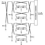 M-level quadrature amplitude modulation (QAM) signal as two half-data-rate amplitude shift-keying signals that occupy the same bandwidth but with an orthogonal phase relationship. A special case exists with quadrature PSK (QPSK) since it is not only four PSK, but also four QAM. Hence, a QPSK signal can be simply generated by a vector modulator realized with two BPSK modulators operating in quadrature, as shown in Figure 8 .
Each biphase amplitude modulator must be operated at a number of different amplitude settings, such as two settings for 16 QAM and four settings for 64 QAM, each with 0° and 180° phase offset, in a push-pull mode. However, unlike the BPSK case, there is no guarantee that the constellation is perfect. While the balance of the circuit is perfect for any pair of diametrically opposite points on the constellation, it is not always the case that the different pairs of constellation points line up together properly. This deviation can be overcome by performing a calibration procedure on the I and Q voltages and storing the results in a lookup table.
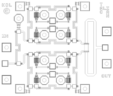 The layout of the balanced vector modulator, which measures 1.25 mm ¥ 1.45 mm, is shown in Figure 9 . It can clearly be seen that by employing the new miniaturized coupler the overall circuit can be greatly reduced in size (total area < 1.85 mm2) and, therefore, cost.
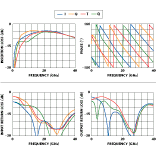 A PC with a DAC card can be used to generate the two sets of complementary pseudorandom baseband signals (I, I_ and Q, Q_). Figure 10 shows the simulated frequency performance of the balanced vector modulator at 30 GHz. The simulated constellation of a QPSK signal at 30 GHz is shown in Figure 11 . It is evident that satisfactory results are obtained when employing the balanced vector modulator, with good input and output matching, and a
  90° phase difference between I and Q, Q and I_, I_ and Q_, and Q_ and I over a wide bandwidth. A phase difference of 180° is also obtained over a wide bandwidth between I and I_ and Q and Q_.
For higher levels of modulation (that is, 16 or 64 QAM), the small imperfections in the performance become more noticeable and the phase imbalance from ideal quadrature can lead to a constellation that is not perfectly square. Figure 12 shows the simulated constellation of a 16-QAM signal without any correction on the control lines of the vector modulator. However, with analog control voltages it is possible to correct these errors by careful adjustment of the I and Q signals. These corrections
 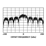 can be stored in a lookup table once the calibration procedure is performed in advance. A DAC then can be used to generate the voltages in real time. The corresponding simulated output spectrum of the vector modulator for 16 QAM at the operating frequency of 30 GHz is shown in Figure 13 .
Conclusion
A common technique for realizing a microwave direct carrier modulator is to employ reflection topology using a Lange coupler with FETs acting as switches on the coupled and direct ports. However, the performance of single-ended modulators is limited at high frequencies. The modulators suffer from both amplitude and phase errors due to the parasitics of the cold FETs. It is possible to remove these amplitude and phase errors using a balancing technique. The balanced modulator using reflection-type attenuators is an extremely robust technique that provides perfect BPSK performance with negligible design effort. However, with the balanced topology, the Lange couplers occupy a large area of the layout. The overall layout can be made much more compact by replacing the Lange couplers with miniaturized capacitor-compensated microstrip parallel-coupled couplers. By arranging two such balanced modulators in quadrature (I and Q), a balanced vector modulator can be realized (with a total area of less than 1.85 mm2), providing near-perfect QPSK performance.
Furthermore, the vector modulator can provide higher level modulation schemes, such as 16, 64 and even 256 QAM. These modulators experience some degradation in performance due to the various process variations and imperfections in the circuit elements. However, these variations can be fine-tuned under the control of analog signals to achieve good constellations, and the corrections then can be stored in a lookup table after calibrating the modulator. Thus, balanced direct modulators have been shown to be very attractive for implementing high performance mm-wave transmitters for digital communications and radar applications.
Acknowledgment
Sonnet em software is a product of Sonnet Software Inc., Liverpool, NY. Series 4 software is a product of HP EEsof, West Lake Village, CA.
References
1. T. Gokdemir, S. Nam, A.E. Ashtiani, I.D. Robertson and U. Karacaoglu, "Millimeter-wave Monolithic-balanced BPSK Modulator Using a Miniaturized Backward-wave Coupler," IEEE MTT-S International Symposium Digest, 1998, pp. 877-880.
2. S.L. March, "Phase Velocity Compensation in Parallel-coupled Microstrip," IEEE MTT-S International Symposium Digest, pp. 410-412.
3. M. Dydyk, "Accurate Design of Microstrip Directional Couplers with Capacitive Compensation," IEEE MTT-S International Symposium Digest, pp. 581-584.
4. G.B. Norris, D.C. Boire, G. St. Onge, C. Wutke, C. Barratt, W. Coughlin and J. Chickanosky, "A Fully Monolithic 4 to 18 GHz Digital Vector Modulator," IEEE MTT-S International Symposium Digest, 1990, pp. 789-792.
Ali E. Ashtiani received his BSEE with honors from King's College, University of London in 1995. He then joined the Microwave Circuits and Devices Group at King's College as a PhD student. Currently, Ashtiani is undertaking research in the area of direct carrier microwave modulators for low cost mm-wave transmitters.
Tacar Gokdemir received his BEng degree in electronic engineering from Queen Mary and Westfield College, University of London. He received his MSc degree in communication and radio engineering from King's College, University of London in 1993. Since 1994, Gokdemir has been working as a research associate on the MMIC Research Team and pursuing his PhD degree. His research interests encompass all aspects of the design and application of MMIC and modeling of multilayer passive MMIC components.
Georgios Passiopoulos received his BSc degree in physics from the National University of Athens and his MSc degree in microwaves and opto-electronics from University College, University of London in 1993 and 1994, respectively. In 1995, he joined the Microwave Circuits and Devices Group at King's College, University of London where he is currently pursuing his PhD degree. Passiopoulos's research interests lie in the area of microwave and mm-wave subsystem design, nonlinear electronics and applied electromagnetics.
Ali Rezazadeh received his PhD in applied solid-state physics from the University of Sussex, Brighton, UK, in 1983. In 1990, he joined the department of electronic engineering at King's College, University of London and currently is a reader in microwave photonics as well as a consulting engineer. Rezazadeh is also the head of the department's Microwave Circuits and Devices Research Group.
Suengil Nam received his BEng degree in microwave engineering from Kyung-Pook National University, Korea in 1983. From 1984 to 1989, he was with the System Research Center of Hyundai Electronic Industry Ltd. In 1989, he joined KTI (Korea Telecom International) and, in 1990, he was dispatched to the University of Surrey for a microsatellite development project. Nam received his MSc from the University of Surrey in 1993 and subsequently joined King's College, University of London as a research associate and PhD candidate. Currently, he is working with the University of Surrey as a research fellow.
Ian Robertson graduated from King's College, University of London in 1984 and then joined the MMIC Research Group at Plessey Research (Caswell) Ltd. In 1986, he returned to King's College as a research assistant working on the T-SAT project's microwave transponder while also working part-time on MMIC receivers for his PhD thesis. From October 1990 to June 1998, he was on the academic staff at King's College and in 1994 he was appointed a reader in microwave engineering. In July 1998, Robertson was appointed to the Chair in Microwave Subsystems Engineering at the University of Surrey.