
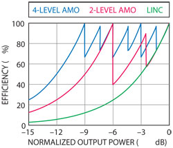
Figure 1 Theoretical efficiency of AMO modulation with four amplitude levels, compared to two-level AMO and "one-level" outphasing (or LINC – linear amplification with nonlinear components).
As wireless communications expand in bandwidth, number of users and geographic coverage, there is a growing demand for higher efficiency in the power amplifier portion of base station transmitters. Wireless power amplifiers consume more than half the total power required to operate a base station. Reducing that consumption through higher efficiency offers several benefits, starting with the obvious benefit of lower operating cost. While a lower utility bill is a significant advantage, less waste heat means reduced equipment cooling requirements and increased reliability. With less concern about temperature rise, a wireless operator has more flexibility in locating the new base stations required to support the dramatic increase in wireless data usage provided by 4G and future generations.
But higher efficiency must be accompanied by the wider bandwidth and high linearity demands of 4G wireless signals. To address this issue, recent startup Eta Devices Inc. is commercializing a technology developed at MIT: asymmetric multilevel outphasing (AMO). AMO combines the high linearity of outphasing with efficiency-enhancing, multilevel, discrete switched drain bias. Discrete switched drain biasing is the key to supporting wide bandwidths while maintaining high efficiency, and is the greatest advantage of this technique over traditional envelope tracking. Figure 1 illustrates how AMO achieves efficiency improvement over outphasing alone.
In any outphasing system, maximum efficiency is obtained from the individual power amplifiers’ performance. In their high power amplifier designs, Eta Devices uses GaN HEMT devices, which have demonstrated practical peak drain efficiencies exceeding 80 percent. GaN technology was selected for its improved performance over existing silicon devices, which struggle to exceed 70 percent peak drain efficiency under similar conditions.
Along with high performance RF amplifiers, the power supply switching system must also be optimized for low-loss switching with minimal transients. System timing is critical, requiring management of the delay in each signal and control path. And once properly synchronized, Eta Devices’ proprietary digital predistortion (DPD) techniques are critical to achieving the demanding adjacent channel power ratio (ACPR) specifications for 4G systems. This architecture has been implemented at a variety of power levels and applications, from 1 W PAs for handsets and WLAN transmitters to 100 W PAs for base stations, and with a variety of semiconductor materials, including GaN, GaAs and silicon.
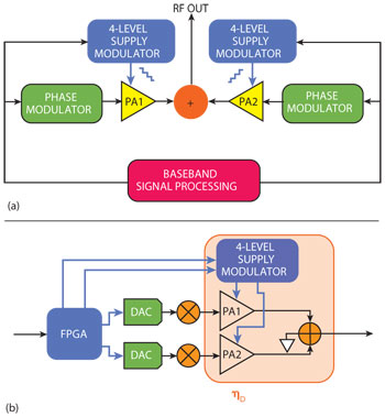
Figure 2 Block diagram of AMO.
AMO VS ET Operation
Two well-known methods for achieving linear amplification with nonlinear power amplifiers are outphasing and envelope tracking (ET). Outphasing uses two phase-modulated amplifiers operating at constant amplitude. The input signal is converted to the proper phases and presented to the amplifiers, whose outputs are combined so that reinforcement and cancellation of the phase components results in a signal that replicates the input accurately. In practice, outphasing requires a power combiner that provides a consistent load for each PA, isolation between the amplifiers, and high power handling capability. These characteristics can be difficult to achieve, especially over a wide bandwidth. Another limitation of outphasing is that signals with high peak-to-average power ratios (low average power output) result in reduced efficiency since much of the amplifiers’ power is wasted and dissipated by a resistive load.
ET splits the RF signal into separate phase angle and amplitude components. The PA operates in saturated mode, typically one of the switching modes such as Class E. Phase modulation is applied to the RF drive while the DC supply to the PA is modulated with the amplitude envelope, thus phase and amplitude are both restored at the output. ET, despite its popularity, is challenged by the increasing bandwidth requirements of 4G and WLAN standards. The crux of the problem for ET is the supply modulator, which must excel in many different aspects of performance. It must handle a lot of power, be extremely efficient, be highly linear, be high resolution, inject very little noise into the system, and support wideband modulation. Modern wireless standards demand increased bandwidth without relaxing any of the other performance demands, putting the future of ET-only solutions in doubt.
The design challenges of outphasing and envelope tracking are addressed by AMO, which combines the most desirable features of outphasing and envelope tracking for improved performance. A block diagram of AMO is shown in Figure 2, where Figure 2a shows the basic functions, and Figure 2b illustrates a typical implementation scheme. It begins with signal processing that delivers phase modulated signals to the power amplifiers, which have multilevel supply modulators. The outputs are combined for an amplified signal with high linearity that maintains the high efficiency of the nonlinear PAs.
While the physics of AMO solutions is conducive to high bandwidth modulation at high efficiencies, it does come at the price of non-traditional DPD solutions which are at the core of this AMO implementation. Although the structure of the DPD is non-traditional, the computational resources required do not differ from that of traditional DPD. Thus, there is no hidden power cost associated with increased digital complexity that would undermine the overall efficiency gains. In summary, AMO allows a tradeoff to address the limitations of outphasing and envelope tracking behaviors, resulting in a system with the best characteristics of each.
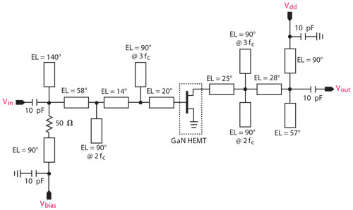
Figure 3 Circuit schematic of the 10 W Class E 1.95 GHz test circuit.2
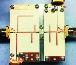
Figure 4 Photograph of the Class E GaN amplifier.
GaN Device and PA Design
The efficiency of the core switch-mode PA determines the maximum system efficiency of techniques like outphasing, ET and AMO. For present day wireless communications amplifiers, most of the highest efficiency production devices are fabricated using GaN processes. For example, the GaN HEMT devices1 used in a prototype developed at MIT2 are specified at 65 percent (3.6 GHz) and > 70 percent (2 GHz) typical efficiency at their maximum saturated output power. The PA circuit diagram is shown in Figure 3, and Figure 4 is a photo of the assembled amplifier. For AMO applications, the PA is designed to have good performance over the range of drain voltages to be delivered by the stepped-switching supply modulator.
Overall Performance
A complete transmitter (see Figure 5) includes several additional system components. Baseband I and Q signals are delivered to a digital predistortion (DPD) and modulation signal processor implemented with an FPGA. In this system, DPD is implemented with a lookup table constructed from measured static nonlinearity of the transmitter for the various combinations of DC levels at the PA. Outphasing channel phase modulation data is delivered to digital-to-analog converters and phase modulators for the two PAs. Amplitude modulation data, with coarse delay correction, drives the supply modulator circuit. RF preamplifiers provide the necessary drive levels, and at the output a combiner sums the PA outputs into a single RF output.
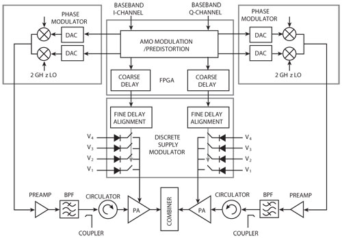
Figure 5 Test transmitter block diagram.
Performance Summary
AMO combines the desired attributes of outphasing and envelope tracking obtained with either method alone. Figure 6 shows efficiency versus bandwidth performance for the four-level AMO test transmitter. The AMO system architecture using Class E GaN PAs, combined with the latest DPD implementation, delivers an average, modulated drain efficiency of 70 percent at 1 MHz bandwidth, with only a slight reduction to 68 percent at 20 MHz bandwidth. Supply modulator losses are included in the efficiency measurement.
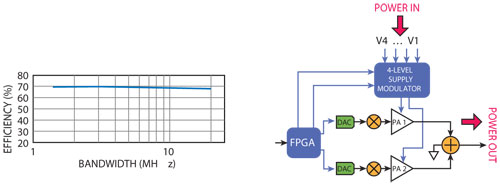
Figure 6 Efficiency versus bandwidth at 2.14 GHz, 100 W peak power, 7 dB PAPR and ACPR > 45 dBc.
Figure 7 shows the spectral energy in adjacent channels with the latest DPD implementation. At 20 MHz channel bandwidth, ACPR performance is > 54 dBc while maintaining 68 percent efficiency. Measured data for efficiency versus backoff is shown in Figure 8. While these devices have 70 percent modulated drain efficiency (including modulator losses) at maximum average output power, the performance at backoff is arguably more important. This is because network operators almost never operate their base stations at maximum average output power. Instead, it is normal to operate at 30 to 50 percent of the maximum. Figure 8 shows that this device system loses only 10 percent efficiency for 10 dB backoff from maximum average power. For a signal with a 7 dB PAPR, this is actually a 17 dB backoff from peak power.
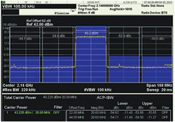
Figure 7 Spectral performance for a 20 MHz BW, 7 dB PAPR transmission. The carrier frequency is 2.14 GHz, and the output power is 100 W peak.
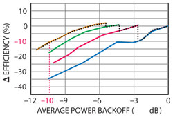
Figure 8 Measured efficiency at backoff (ACPR > 45 dBc). The four individual drain voltages are shown, with the dotted line illustrating how 4-level AMO achieves system efficiency over the entire power backoff range.
This technology continues to expand its capabilities, focusing on support of both LTE and MC-GSM, enabling software-defined radio, and meeting the challenges of expanded bandwidth standards such as WLAN.
References
- CGH40010 data sheet, Cree Inc., available at www.cree.com/rf/.
- P. Godoy, S.W. Chung, T. Barton, D. Perrault and J. Dawson, “A Highly Efficient 1.95 GHz, 18 W Asymmetric Multilevel Outphasing Transmitter for Wideband Applications,” IEEE International Microwave Symposium Digest, June 2012