
A CMOS Fractional-N PLL IC at Microwave Frequencies
Peregrine Semiconductor Corp.
San Diego, CA
Designers of modern microwave terminal systems are faced with a global competitive market that is leading to a greater emphasis on power efficiency, size and cost. Component vendors must respond to these needs with not only lower cost solutions for today, but also with a future road map to continuous power and cost savings.
While other electronic systems can use low cost, high integration CMOS-based IC products, the microwave system designer has had no CMOS option until now. Currently, all microwave IC component suppliers rely on expensive, power-hungry technologies such as BiCMOS and GaAs. CMOS technology has come to dominate the semiconductor industry because of its cost effectiveness. Therefore, an ideal RFIC solution to these cost- and power-reduction demands would be a CMOS process technology with RF capabilities.
Despite their cost and power-saving benefits, CMOS processes have been able to yield components in the several hundred megahertz (IF) region only — never in the 1 to 2 GHz region. This limitation is due to the fact that, in standard CMOS processes, circuit elements are placed on a silicon semiconducting substrate creating two problems that cannot be addressed by reducing the size of the transistors through lithography improvements. The first problem is the parasitic capacitances between the circuit elements and the substrate. These capacitances lead to reduced inductor performance, slower digital circuits and energy loss into the substrate. The second problem is that the conducting substrate creates an electrical coupling between circuits. Such coupling means that sensitive RF circuits cannot be isolated from noisy receiver sections such as analog-to-digital converters and digital logic. Isolation is imperative for RF and baseband integration.
What would happen if CMOS was available on a cost-effective insulator? The unique, patented ultra-thin-silicon (UTSi“) CMOS process represents just such a CMOS technology offering a cost-effective isolator in a CMOS process. Figure 1 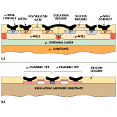 shows cross sections of an inverter circuit implemented in a typical submicron bulk CMOS process and in the UTSi process. The basic transistor structures are similar except that wells, well contacts, isolation regions and substrate contacts are not required in the UTSi version.
UTSi CMOS has been perfected and is a mass-volume, qualified process that can be manufactured in a standard, unmodified CMOS fabrication facility. Unlike BiCMOS or GaAs, UTSi CMOS takes advantage of decades of advances in CMOS manufacturing cost effectiveness. In fact, the process is even more simple than standard CMOS.
UTSi is a silicon-on-insulator CMOS process with roots in decades of military research. With its inherent speed, isolation and packing-density advantages over other CMOS processes, UTSi makes CMOS IC design available to today’s RF designers. The UTSi process not only produces phase-locked-loop (PLL) ICs with elite specifications, but it is also capable of producing useful high Q onboard inductors as well as RF mixers and switches with good linearity on a low cost sapphire (crystalline alumina) substrate.
The new model PE3282 dual fractional-N PLL, the world’s fastest all-CMOS PLL, is a specific example of the advantages of UTSi CMOS. Competitively priced vs. current BiCMOS products, the PLL offers low spurious output levels. The PLL also costs less to produce than equivalent BiCMOS solutions and delivers operating frequencies of up to 1.6 GHz.
PLL Specifications
The PE3282 dual fractional-N PLL includes two complete PLLs, a three-wire serial data interface and a multiplexed output to monitor internal states, including lock detection. Each PLL contains a fractional-N main counter chain, a reference counter, a phase detector and an internal charge pump with on-chip spur compensation.
Each fractional-N main counter chain includes an internal dual-modulus prescaler, supporting counters and a fractional accumulator. The fully insulating substrate of the UTSi CMOS technology provides inherently latch-up-free operation and optimal electrostatic discharge protection. The PE3282 provides 2 kV human body model protection on all pins, including the high frequency prescaler input and the charge pump. This robustness enhances final board yield in a mass-manufacturing environment. Similar protection levels are often missing in RF PLLs built using older process technologies such as BiCMOS.
Counters
The basic-N counters use a standard combination of a dual-modulus prescaler, an A counter to control the prescaler modulus and a B counter that resets all of the counters when it reaches terminal count. The fractional function is supplied by a five-bit accumulator and incrementer that cause the N counter to count by N + 1 each time the accumulator overflows (which happens every 32/I cycles of the N counter where I is the increment value). This combination forms the fractional-N counter. If the increment is set to 1, the counter will divide by N for 31 cycles. However, when the accumulator overflows on cycle 32, the main counter chain will divide by N + 1. Across the cycles, the main counter will divide by an average of N + 1/32.
Improved phase noise is a consequence of the higher comparison frequency fc and lower values of N used with the fractional architecture. The PE3282, shown in Figure 2 , has a  maximum fractionality of 32, yielding an improvement in phase noise of approximately 15 dB. No special software is required to access this performance, and the improvement is inherent to the PE3282’s architecture.
Internal Spur Compensation
Traditionally, a fractional-N architecture system’s advantages come at the expense of FM spurs that appear on the VCO output. The problem is that the alternate counting by N and N + 1 produces considerable FM modulation, which results in large spurs. Without a compensation technique, these spurs act as unacceptable sidebands.
Some fractional devices available currently remove spurs using analog techniques that are power hungry and sensitive to component and voltage variations. These traditional spur compensation methods require adjustment of current-setting resistors to compensate for device-to-device variations in the charge pump current. Such outdated current-compensation methods are accurate only for one value of N and tend to lose calibration across temperature. However, the PE3282 differentiates itself from PLL competitors with a novel on-chip fractional spurious output compensation that allows suppression of the fractional spurs with no external components and no tuning. This unique compensation technique (for which a patent has been filed) allows the system designer to take advantage of a fractional architecture without the headache of tuning the finished circuit or the risk of compensation performance degrading across voltages and temperature variations.
For the first fractional spur, as shown in Figure 3 ,  the PE3282 typically achieves levels of suppression better than –70 dBc. The good spur reduction of the PE3282 helps in transmission applications by significantly lowering interference in adjacent channels and aids in receiving applications by improving adjacent-channel rejection.
Applications
With an all-CMOS construction, the PLL is a suitable solution for high volume wireless communication applications, including cellular and cordless telephony, paging, analog or digital television tuners, and satellite direct-broadcast receivers. The PE3282 is a monolithic, dual-frequency synthesizer intended for specific application as the local oscillator for the RF and first IF of dual-conversion transceivers.
Future Custom Integration
Still under development are a wide range of RF and digital test circuits that show dramatic performance and cost advantages over current semiconductor processes. A few such performance parameters have been measured and are listed in Table 1 .
|
Table 1 - Typical UTSi-Fabricated Component Performance | |||
|
Parameter |
Test Circuit Performance |
Conditions |
Comments |
|
Spiral inductor Q |
14 |
1 GHz |
25 nH |
|
Spiral inductor self resonance |
> 10 GHz |
|
25 nH |
|
Unloaded logic inverter delay |
< 75 ps |
1 V |
0.5 µm drawn gate |
|
SP2T switch insertion loss |
0.65 dB |
1 GHz |
|
|
SP2T off port isolation |
42 dB |
1 GHz |
|
|
Mixer IIP3 (LO = 0.05 to > 1 GHz) |
> +20 dBm |
RF = 1 GHz |
|
|
Transistor fmax |
32 GHz |
3 V |
0.7 µm drawn gate |
|
Transistor ft |
12 GHz |
|
0.7 µm drawn gate |
|
Low noise amplifier noise figure |
1.7 dB |
1.4 GHz |
gain > 9.5 dB |
To properly support any process for RF integration, accurate device models are necessary. Commercially available packages for CMOS simulation are inadequate and have numerous limitations for RF applications. In recognition of these facts, significant investments have been made to create and refine sophisticated UTSi device models. For example, linearity at microwave frequencies is a key parameter that is not addressed by existing modeling solutions. The new UTSi models will specifically predict distortion and other key parameters needed for advanced RFIC designs. Through such developments, the UTSi process offers custom, high integration RFICs, including a low noise amplifier/switch/PLL/mixer RF chain integrated onto a single die. Such ICs will provide system cost/performance advantages that, in turn, will put the designers who use the components ahead of the competitive treadmill.
The total integration of all semiconductor elements of a microwave terminal onto a single die is known as the Microcommunicator“ concept. Analysis of current process technologies and UTSi CMOS shows that UTSi is a good, and perhaps the only, process technology that enables such a single-chip vision. Microcommunicator products truly will provide RF system designers with the ultimate in cost, power and size reductions, all of which are needed to succeed in today’s competitive global marketplace.
Conclusion
The PE3282 dual fractional-N PLL IC offers high performance dual-IF/RF PLL capability by utilizing the patented all-CMOS UTSi process. The unit’s fractional architecture yields up to a 15 dB improvement in phase noise for a given choice of output frequency and step size. The PE3282 also offers 70 dB suppression of fractional spurs without tuning and without additional external components. The unit is qualified to full commercial specifications and will be available for production during the third quarter of this year. Samples and advance datasheets are available currently. Prices start at $2.50 per unit for orders exceeding 100,000 units.
To speed the evaluation of the PE3282, the PE3282-EK evaluation kit containing a 2.75" x 3.25" surface-mount board, and schematic and layout information are also available. Using a standard PC with either Windows 3.1 or Windows ’95 installed, the PE3282-EK simply plugs into the parallel printer port. This evaluation kit enables the end user to run the PE3282 through its paces quickly and reliably. The PE3282-EK kit is available immediately for $399.
Peregrine Semiconductor Corp., San Diego, CA (619) 455-0660.