
Several Austin, Texas companies were founded on the fundamental idea of applying mixed-signal CMOS technology to analog design challenges that traditionally used complicated and expensive semiconductor technology or discrete analog components. Repeatedly, once a viable CMOS solution was introduced, the market made a wholesale shift to the CMOS implementation. In the case of Javelin, the technical challenge was to design a linear cellular power amplifier (PA) in standard CMOS technology when existing suppliers are using proprietary GaAs technology. Several companies had already invested millions of dollars and more than a decade of design effort attempting to develop a cellular PA in CMOS, but they were unable to meet stringent 3G performance requirements in a CMOS implementation. Therefore, Javelin was also faced with the business challenge of proving the capabilities of CMOS for 3G applications and convincing a Tier I handset manufacturer to qualify a new PA supplier.
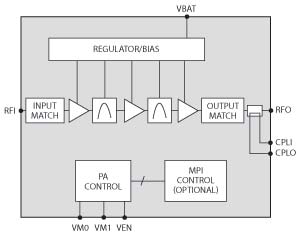
Fig. 1 JAV550X architecture.
Javelin sees 3G as the entry point for CMOS to become a mainstream process technology for the cellular PA. The requirements for a 3G PA are very demanding in terms of performance (efficiency, linearity and noise), reliability and also in having a high yielding, large capacity manufacturing supply chain. Javelin is the first company to produce a CMOS 3G PA that does not compromise any of these requirements. To break the GaAs PA monopoly in the 3G handset, Javelin developed an innovative mixed-signal architecture offering performance advantages while meeting or exceeding all stringent industry requirements. The innovative architecture provides an inherent bandpass response to minimize receive noise for 3G and other radios in the handset, while delivering excellent efficiency across the wide range of required output power levels. Because Javelin’s PA is a 100 percent CMOS implementation, supply limitations are eliminated.
Javelin’s PA was modeled and designed to meet the output power and linearity requirements of the 3GPP UMTS standards. The PA has a bandpass architecture that includes an input matching network, tunable bandpass filtering between each amplifier stage and an output matching network (see Figure 1). The PA also integrates complete circuitry for power regulation, PA bias and power control.
The integrated bandpass filtering can have a significant benefit in UMTS Band I (1920 to 1980 MHz transmit and 2100 MHz receive) applications, which is supported by the Band I PA. Typically, the transceiver transmit noise in Band I is filtered with a surface acoustic wave (SAW) filter between the transceiver RF output and PA RF input. With the bandpass filtering in this design, the SAW filter can be removed, saving both cost and board area. The result is a bandpass response with low out-of-band skirts that reduces receiver noise (see Figure 2).
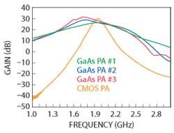
Fig. 2 Bandpass filter response for various PAs.
In the situation where transceiver noise is already low and a TX SAW is not required, the bandpass filtering provides additional margin for ease of implementation as well as manufacturing margin. Even with a low-noise transceiver and a traditional PA of any band, the duplexer (DPX) must maintain greater than 45 dB isolation for acceptable receive sensitivity (desense). This level of isolation from the DPX is a challenge, and very careful PCB layout is required for the DPX and surrounding components. Javelin’s PA reduces the DPX isolation requirement by the TX-to-RX gain difference. In this case, the DPX isolation requirement is reduced by more than 10 dB.
Also, particularly in smartphones, the bandpass filtering can provide benefits to overall performance. Smartphones contain multiple wireless interfaces, such as Wi-Fi, Bluetooth and GPS, which have low receive signal power levels. The bandpass filtering reduces interference with these other wireless interfaces and helps to lessen the RF design challenges within the smartphones.
Javelin offers a family of CMOS PAs covering the most popular UMTS bands including solutions for Band I (1920 to 1980 MHz), Band II (1850 to 1910 MHz), Band V (824 to 849 MHz) and Band VIII (880 to 915 MHz). Javelin’s architecture ensures consistent performance by using a patented design with tunable filtering to optimize performance and maximize manufacturing yield. The result is a highly manufacturable, high yielding device that consistently meets stringent specifications. For example, the JAV5501 offers 26.5 dBm maximum linear output power in high power (HP) mode, 28.5 dB typical gain in HP mode, -42 dBc ACLR with ±5 MHz offset, -148 dBm/Hz noise in RX band with 190 MHz offset and 1.5 percent typical error vector magnitude (EVM).
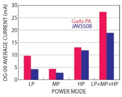
Fig. 3 Weighted average current in each mode according to the DG-09 average current definition.
All of Javelin’s PAs offer low average current with a direct connection to the battery. The JAV5505 and JAV5508 lead the industry with DG-09 average current below 19 mA, which is over 30 percent lower than competing devices. At specific low output power levels, PA current can be reduced by over 60 percent. The low average current is achieved using typical low power (LP, -47 to 6 dBm), medium power (MP, 6 to 15 dBm) and higher power (HP, 15 to 26 dBm) switch points, and without the additional cost and board area of a switch-mode power supply (SMPS) DC/DC converter to control the PA supply voltage. Figure 3 shows the current levels that are the weighted average currents in each mode, according to the DG-09 average current definition.
Because the PA delivers significant power and is connected to the battery and the antenna, Tier I handset manufacturers require not only high performance, but also high quality and reliability. In Javelin’s case, standard CMOS technology becomes a major benefit, because a monolithic CMOS approach leads to the highest manufacturing line yield and maximizes long term reliability in the field. Javelin’s PA family utilizes the world’s largest capacity process node of the CMOS supply chain combined with industry standard high-volume packaging technology to offer world-class quality and reliability, including a very high tolerance to electrostatic discharge (ESD) events. Javelin PAs are rated at 6 kV on RF pins and 3 kV on all other pins which is critical to manufacturing quality and reliability. Additionally, Javelin PAs can withstand driving full output power into a short circuit or open circuit without damage, which is critical to field quality and reliability.
The 3G smartphone market is an ideal starting point for a CMOS PA, as 3G is forecasted to be the largest segment of the mobile phone market over the next five years. Comparatively, the Long Term Evolution (LTE) market segment is currently small on a worldwide basis, but continues to experience rapid growth. Javelin’s mixed-signal CMOS architecture is well suited for LTE. The transition to LTE will create additional PA design challenges while the higher peak to average ratios will require advanced architectures with more integrated intelligence and CMOS is well suited for this trend. As an example, the MIPI RF Front-End (RFFE) control interface, supported on Javelin PAs, is an industry standard digital communications interface which was defined to enable the integration of advanced features into the PA. In the future, this digital interface to the PA can be used for advanced power control and envelope tracking techniques. Thus, Javelin sees the CMOS PA trend continuing from 3G to LTE and beyond.