

OnScale is a leader in Cloud computer aided engineering (CAE), running multi-physics solvers on its Cloud HPC platform running on Amazon Web Servers. Their platform helps engineers to accelerate innovation for next-generation products such as 5G smartphones, IoT, biomedical devices and driverless car products by greatly reducing the solving time with massive computing power and using optimized algorithms. It also allows companies to only pay for the services they need, when they need them, reducing overall costs for CAE. Their pricing is very aggressive with free individual single user service (up to 10 core hours), $300/month for Pro level individual user (up to 50 core hours), and $1000/month for team of 10 users (up to 200 core hours).
Filters for 5G networks are a critical component as more frequencies are used and the spacing between them is reduced. Therefore OnScale is focusing on technologies such as FBARs, SMRs, and TC-SAWs as designers are engaged in bringing new designs to market quickly. OnScale maintains that traditional design and optimization practices that are heavily reliant on trial-and-error prototyping so will not be sustainable in this new, fast-paced market. Consequently, engineers are adopting FEM approaches to virtually prototype devices and explore massive new design spaces to find optimal and robust solutions using their platform.
The scale of Amazon Web Servers enables massive solving power coupled with OnScale’s faster solvers can dramatically reduce design time and improve the chances of first pass success with robust modeling of all of the design alternatives available. Sometimes not all design scenarios are investigated due to time constraints but using their massive solving power, this is no longer a significant limitation.
As an example from their web site, film bulk acoustic resonators (FBARs) can often exhibit spurious modes across the pass band which is one of design challenges an RF engineer faces. OnScale gives engineers the ability to quickly prototype a design to understand how effective it is removing these modes.
The 3D FBAR model provides a simple starting structure consisting of a piezoelectric active layer (Aluminum Nitride) with Molybdenum electrodes on a silicon substrate.
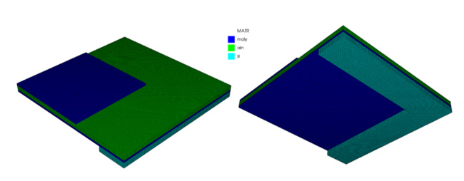
Model Schematic
Parametric Variables
The base model allows the following design variables to be adjusted. By default electrode thickness and electrode aspect ratio are set as design variables to be swept (indicated by *).
|
Parametric Variable |
Description |
Default Value |
|
aln_thk* |
Thickness of AlN piezoelectric layer |
800 nm |
|
targ_wid* |
Width of top electrode |
30 um |
|
sub_out |
Distance from end of cavity to end of AlN |
5 µm |
|
cav_out |
Distance from end of electrode to end of cavity |
5 µm |
|
cav_thk |
Thickness of cavity |
1 µm |
|
elec_bot |
Bottom electrode thickness |
400 nm |
|
elec_tot |
Top electrode thickness |
400 nm |
Outputs
A wide range of outputs can be generated, including:
- Electrical Impedance
- Quality Factor
- Mode Shapes (Harmonic Analysis)
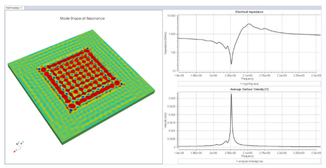
Post Processor Outputs
Runtime Statistics
|
Model Size |
184093 elements |
|
Solve Time |
343 secs (16 CPUS) |
|
Core Hours |
1.54 |
|
Memory Usage |
269 MB |
|
Recommended CPU Configuration |
16 CPU |
This is a very interesting approach and the industry is seeing more companies getting an advantage in the market with cloud or AI enhanced services. We have seen Optimal+ and GradientOne doing cloud data acquisition and analysis for semiconductor measurements and NI AWR offering cloud design services for Antennas with their AntSys product so we will follow this trend as it continues.