

PCB design is increasingly becoming a challenging task on account of several factors including miniaturization but also the fact that it needs to have a presence of digital, mixed as well as radio frequency or what is popularly known as RF signals. As a thumb rule, a PCB is called a RF PCB when the frequency of signals involved, exceed 100MHz. RF PCB is one of the fastest growing sectors in PCB manufacturing. With the proliferation of electronic devices such as smartphones, sensors, robotics and more, the demand for these high frequency boards is in the increase.
For RF PCBs, however, you need a whole new approach to layout as well as routing, as opposed to low frequency PCBs. In fact, for RF PCBs, it is important to look at the entire circuit as a distributed parameter system. PCB Designers face a lot of challenges while PCB Fabrication. Some of the challenges that designers face when it comes to RF PCBs include:
- Capacitive coupling between signals
- Electromagnetic Interference
- Impedance Control
- Thermal Management
Let us look at some of the factors to consider and guidelines to follow in some detail when routing radio frequency printed circuit boards.
Impedance Matching
This is an extremely important factor to consider when it comes to RF PCBs. In the absence of impedance matching the PCB is likely to suffer from power losses as also signal reflections along the PCB traces. The impedance of the load needs to be the complex conjugate of the source impedance. Therefore, in order to maximize the transfer of power, impedance matching is required.
Since most systems and radio frequency modules have an impedance of 50 Ω, it is preferable that the traces of an RF printed circuit boards have an impedance of 50 Ω. The two types of traces commonly used on PCBs are a) Microstrips- In this case, traces are placed on the outer layers of the PCB b) Striplines- Here, the trace lies between two ground planes.
To ensure that traces remain impedance matched, it is important to ensure the following:
- Use an impedance-controlled design with the layer stack. This will ensure that traces routed in the signal layers have a defined value within a specific tolerance.
- A common impedance matching topology is the L-network. This network uses a capacitor and inductor, two capacitors or two inductors to match the 50 Ohm impedance.
- It is also important to choose the right SMD component size. A commonly followed rule involves selecting components whose width is comparable to that of a trace with an impedance of 50 Ω. This will take care of impedance matching issues between the trace and the component pads.
Some of the other things to keep in mind when it comes to impedance matching, include:
Skin Effect Loss- At higher frequencies, electrons flow along the outer surface of the conductor. This is commonly known as the skin effect. At the trace, a small area is used to funnel electrons. The funnel, however, can also trap some electrons. In turn, their signal energy is converted into heat or what is commonly known as the skin effect loss. Proper impedance matching can go a long way in minimizing this loss.
Keeping Line Lengths Low- Long lines carrying RF signals can lead to signal loss. As a thumb rule the line should be 1/20 of the wavelength. The critical signal length is 1/16 of the wavelength.
Reducing Capacitive Coupling
Capacitive coupling also known as electrostatic coupling is the transfer of electric energy between two insulator-separated conductors. For example, if two copper traces are kept close to each other, the energy on one trace will be transferred to the other. 3 common ways to prevent capacitive coupling in the PCB (printed circuit board) layout include:
- Increasing distance between traces- Capacitance is inversely proportional to the distance between terminals. Therefore, higher the distance, less the capacitive coupling.
- Shielding high frequency traces with a ground terminated copper strip- The ground strip acts as a shield and ensures that the charge is prevented from coupling to other traces.
- Keeping traces short, as long traces increase the area of the conductor, which in turn increases capacitive coupling.
Electromagnetic Interference (EMI)
Electromagnetic interference (EMI) is electromagnetic energy that disrupts the signaling in an electronic device through radiation or induction. From the static on the radio, to that buzz we hear when you bring a cell phone near audio equipment, Electromagnetic interference (EMI) is all around us.
It is the electromagnetic compatibility or EMC, which is the ability of the electronic system to operate within an electromagnetic environment satisfactorily without generating intolerable EMI that RF PCBs (Radio Frequency Printed Circuit Boards) need to aim for.
When a device deviates from defined standards, EMI dominates the system performance. It is, therefore, important to control EMI during the early phases of the PCB design.
The common techniques to reduce EMI in PCBs include:
Ground Plane
Common best practices for reducing EMI with ground plane include:
- Using a multi layered board
- Avoiding long return paths as they result in mutual coupling resulting in crosstalk.
- Connect split ground planes at a single point
- Connect decoupling capacitors to ground plane
Trace layout
Common best practices for trace layout include:
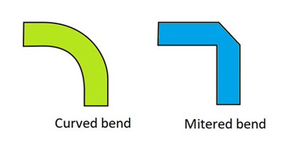
- As a general rule, transmission lines should be kept straight. However, when it is necessary to switch direction, it is best to follow the thumb rule of the radius of curvature being equal to at least three times the trace width. If it is not possible to place a curved trace, the next best option is for the routing to follow a rounded right angle.
- In case of multiple layers, it is important to use vias wisely when Multilayer PCB Fabrication is in progress. On account of parasitic capacitance and inductance in the vias, there can be an impedance mismatch between via and trace, which creates reflections. Where vias cannot be avoided, ground vias should be placed close to signal vias. In differential pairs, when vias cannot be avoided, the same number of vias should be put in both traces.
- Keep return paths short
- Route differential traces as close as possible
Arrangement of components
Best practices for component layout include:
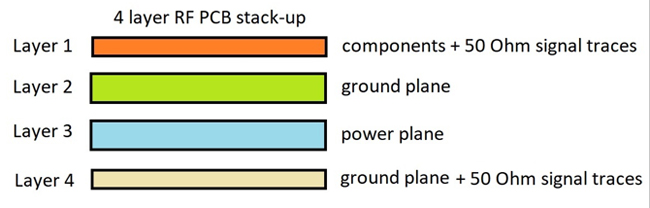
- Keeping analog circuits separate from digital circuits to avoid crosstalk. Taking advantage of multiple layers as well as using separate grounds are some of the options. The number and the type of layers impact your routing decision. If you have a double-sided printed circuit boards you need to be extremely careful about the routing given the fact that the space available is limited. On the other hand, if you have a four-layer PCB, you have better space to create ground and power planes besides offering greater strength to the circuit on account of its thickness.
- Isolate high-speed components- As a thumb rule, the faster and smaller the component, the higher the EMI.
EMI (Electromagnetic Interference) Shielding
Shielding is a mechanical technique that uses conductive or magnetic material to prevent EMI. Some components that naturally produce EMI can be shielded using a Faraday cage. Simply put, it is an enclosure made up of a conductive material that can block RF waves. Shielding protects signal transmission from external noise and prevents information loss.
In addition, cables that carry analog and digital signals can create EMI issues. Shielding these cables ad connecting them to the ground, helps prevent Electromagnetic Interference.
Heat Dissipation
Thermal Management is a very key aspect when it comes to RF PCBs. Left unchecked, it can lead to catastrophic failures of the system as also shortening of their lifespan.
Heat that is generated within a PCB material needs to flow away and be dispersed. Some aspects that can help with thermal management include:
- A very important part is played by the choice of PCB material. If the PCB material has a high value of thermal conductivity, there is not only better heat flow the circuit also operates at higher power levels.
- The length of the thermal path on the PCB needs to be as short as possible
- The design of the circuit also helps in thermal management. For example, the use of plated through holes can dissipate heat from an active device. If there are multiple PTHs, they can act as thermal paths assisting in the dissipation of heat.
- It will be ideal to separate heat-generating components from heat sensitive ones. If the PCB is mounted vertically, it is also prudent to place heat-generating components on the top.
With the above best practices in mind the PCB designer can win the fight to maintain good signal integrity when it comes to Radio Frequency PCBs.
Whenever there is a requirement to manufacture advanced radio frequency printed circuit boards, one needs to maintain the signal integrity with a complete set of circuit simulation tools, PCB routing and circuit board layout tools, design tools to reach the target. The best way is to get a help of various available tools whether you need to layout a noise amplifier for signal collection, radio frequency power amplifier to broadcast signals, or complex interconnections.
There are many leading printed circuit board manufacturing companies available who have a best team of circuit board designers, layout engineers, fabricators, assemblers and quality control team who can help you to deliver the standard radio frequency printed circuit boards.
Suresh Patel has worked as a Sales Engineer and other management roles at Mer-Mar Electronics. He brings 25 years of experience in printed-circuit-board sales and technical client service and managing business.