
 Today’s circuit designers are tasked with creating a high performance product that will stand out in a market crowded with competition.
Yet relying on standard 50 Ω MMIC “gain block” devices makes it increasingly difficult for the RF designer to differentiate the specified performance of their radio product. One solution addressing this dilemma is found in discrete devices that have excellent performance and reliability, and can be easily optimized for an exact fit in a given application.
A heterojunction field effect transistor (HFET) is an excellent device for realizing efficient, reliable solutions with the high gain and high linearity needed by communications infrastructure manufacturers. Designers can optimize the performance of their system by using a discrete HFET transistor and enjoy the benefits of a mature and reliable GaAs process technology.
TriQuint has manufactured HFET devices for more than a decade and has optimized this GaAs process to provide industry-leading performance and durability. With a strong legacy of traditional HFET die and foundry products, the company is now creating a family of plastic-packaged products designed for use in a wide variety of end products. TriQuint’s HFET GaAs process can operate with higher junction temperatures than other competitive solutions while still meeting the stringent MTTF goals that are common in applications such as cellular base stations, cable infrastructure and broadband wireless communications networks. Using the performance advantages that can be achieved with an optimized discrete transistor solution, circuit designers can now leverage the devices’ key benefits to meet the demanding needs of their applications.
Design Basics
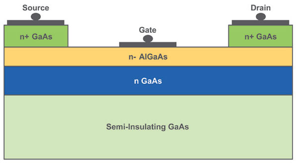
An HFET is constructed by creating a junction between two materials that have differing band-gap energies, commonly referred to as a ‘heterojunction.’ In practice, a moderately thick layer of lightly-doped AlGaAs is placed on top of a thick layer of doped GaAs forming a heterojunction where the two layers meet (see Figure 1).
The HFET uses the wide band-gap AlGaAs layer effectively as an insulator. As current flows in the doped GaAs layer it is modulated by the gate situated on top of the AlGaAs layer.
This structure allows HFET devices to operate at very high frequencies with high gain while providing both superior linearity and operating voltage range.
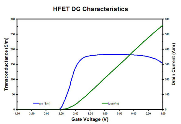
The highly linear transfer characteristic of the HFET is illustrated by the flat transconductance curve of Figure 2.
Market pressures have pushed more and more designers to use MMIC gain block devices instead of discrete parts in order to reduce time-to-market turnarounds. However, the cycle time advantage found in using these types of devices is offset by lower performance when compared to a well-optimized discrete solution. In cases where a designer is searching for the best possible performance and can afford the small amount of incremental time needed to optimize a discrete solution, the payoff can be significant. Typically, a discrete solution will be as good as or better than an MMIC solution in all RF parametric areas, and will have a significant advantage in terms of efficiency.
Characteristically high gain and excellent linearity make HFET devices a stand-out choice for highly linear applications that need to operate efficiently. Examples of such applications include use as a pre-driver or in the driver stages of cellular base station amplifiers, or as power amplifier stages for other broadband applications such as Wireless Local Loop (WLL), WiMAX, or enterprise-class WLAN access points or bridges. The high linearity and PAE of HFET devices also make them well-suited for use in downstream cable amplifiers.
HFET devices are predecessors of the more complex PHEMT (pseudomorphic high electron mobility transistor) devices that are also available today. Compared to PHEMT, the HFET has a lower gate-source capacitance, making it easier to match due to higher input impedance. Additionally, the simplicity of the HFET structure (compared to PHEMT) means that parametric values are typically better controlled, allowing circuit designers to realize lower variances in key system performance parameters such as gain and OIP3.

TriQuint is releasing a pair of HFET transistors in industry standard SOT-89 packages. The devices’ performance specifications are summarized in Table 1.
One product is a 0.5 W nominal (P1dB) device and the other a 1 W nominal device. Both parts achieve excellent gain for a single-stage device, approximately 20 dB maximum at 1 GHz.
The devices are highly linear, with typical output third-order intercept points of 40 and 43 dBm for the TGF2960-SD and TGF2961-SD devices, respectively.
As can be seen in the table, drain efficiencies as high as 62.5 percent are achievable at P1dB.
The high gain and linearity of these wideband devices across a sizeable range of output power can be seen in the performance graph shown in Figure 3.

This result was measured on an evaluation board that was tuned for the 2.14 GHz frequency band. The evaluation board layout can be seen in Figure 4.
TriQuint’s 0.5 μm HFET process is widely acknowledged as extremely rugged. This depletion mode process technology is appropriate for a wide range of applications.
An advantage of HFET compared to competing PHEMT technologies is the ability to operate with a higher channel temperature: up to a 175°C for a median lifetime of over 110 years. This makes it well suited for high reliability applications, or challenging thermal environments such as outdoor convection-cooled masthead amplifiers.
The TGF series of discrete HFET devices is fabricated in an ISO9001 facility with 100 percent lot traceability and full statistical process control. This family of devices is treated with a surface passivation layer to ensure reliable operation in non-hermetic environments.

Conclusion
Engineers looking to wring the last dB of performance from a design in order to differentiate their product from the ‘pack’ should consider the robust performance offered by TriQuint HFET devices. A discrete solution will typically function as well or better than an MMIC design in all RF parametric areas while providing a significant efficiency advantage.
Heterojunction FET devices have a number of appealing characteristics for a wide range of communications applications. They can operate to very high frequencies, have excellent gain and linearity over the entire frequency range, and operate very efficiently. HFETs are dependably robust and are able to operate reliably in challenging thermal environments. Compared to competing PHEMT technologies, the HFET typically offers better MTTF reliability, higher breakdown voltages and excellent linearity.
TriQuint has a broad portfolio of HFET transistors designed with gate peripheries ranging from 1.2 to 24 millimeters. The TGA292x-SG family of high power packaged and pre-matched HFET devices are designed for specific frequency bands ranging from 2.6 to 6.0 GHz. The new general-purpose TGA2960-SD and TGF2961-SD HFET devices are designed to complement the existing product line and are both housed in Green/RoHS-compliant plastic SOT-89 packages. These devices exhibit output powers at 1 dB compression of 0.5 and 1 W, respectively.
Both the TGF2961-SD 1 W device and the TGF2960-SD 0.5 W device are now available for sampling. High performance GaAs HFET devices with well-documented robustness are now easier to use than ever before, with industry standard SMT packaging and tuned evaluation boards available for commonly specified frequency bands. For more information, please e-mail: info-broadband@tqs.com.
TriQuint Semiconductor Inc.,
Richardson, TX (972) 994-8456,
www.triquint.com.
RS No. 302