Figure 5 shows the simulated S-parameters of the proposed design. It shows return loss values greater than 15 dB from 128.9 GHz to 176.9 GHz. With this 31.4 percent fractional bandwidth, the insertion loss is 0.43 dB at the center frequency, dropping only to 0.64 dB in the upper frequency corner. The simulation verifies that the design meets the D-Band loss flatness requirements, which are critical for very wideband signals.
Feeding Options
The proposed transition allows a MMIC to be placed on either side of a waveguide feed and connected to that MMIC. This is a key advantage of this technique and it is enabled by the V-shaped slot configuration, along with the excitation of the quasi-TE10 mode. This mode evenly distributes the currents between the bottom and the top metal layers. With a symmetric field distribution, the output can be on either layer with a 180-degree phase shift. This provides additional implementation possibilities:
- Basic configuration: 50 Ω feeding line and waveguide transition are on the same side
- Flippable configuration: 50 Ω feeding line and waveguide transition are on opposite sides
- SIW fed configuration: Can exploit a single V-shaped slot for SIW feeding
- Planar configuration: If there is no advantage to connections on top and bottom, performance can be improved by eliminating the V-shaped slots.
PARAMETRIC STUDY
D-Band circuits involve very small features compared to standard RF and microwave applications. The resolution of the standard photo etching process may become a limiting factor for performance. This transition requires micrometer resolutions that are challenging up to 175 GHz. This section studies the effects of different manufacturing tolerances and assembly alignments of different parts can have on electrical performance. Design robustness is important for industrial readiness and component yield. This section investigates four design parameters.
Substrate Thickness
Unpredictable thickness variations can result from the lamination of the alumina substrate. The 0.005 in. alumina substrate may have a thickness tolerance variation of ±10 percent or 0.0005 in. Simulations show a frequency shift up to 10 GHz at the maximum substrate thickness variation. Even though return loss and insertion loss flatness do not change much, this is a significant change in frequency.
Dielectric Constant
The dielectric constant, εr, also has a tolerance. In this study, the dielectric constant of alumina was allowed to change by ± 10 percent to assess design robustness. The frequency response shifts by 0.5 GHz for every 0.1 change in the dielectric constant. The loss patterns appear to be unaffected by this dielectric change.
Waveguide Alignment

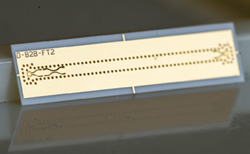
Figure 6 Back-to-back D-Band flippable transition sample.

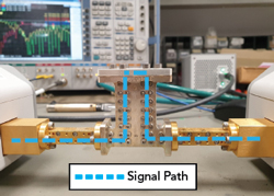
Figure 7 Test circuit measurement setup.

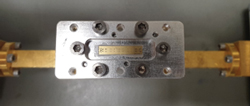
Figure 8 Top view of the measurement setup.
The stepped transformer that matches the WR-06 connection to a custom-sized transition must be carefully positioned on the transition since misalignment influences performance. To investigate position sensitivity, the waveguide transformer has been incrementally shifted in 25 µm steps along X- and Y-directions. At shifts up to 50 µm, the matching is degraded, but the return loss is still less than 10 dB in the 130 to 175 GHz band. However, the insertion loss exhibits a deep notch at 156 GHz.
Via Hole Position
The metallized through-hole via location is crucial for controlling the operational bandwidth and the matching response. Even if they are laser drilled, vias have a poorer tolerance than photo-etched traces. The via position can shift by ± 25 µm and the inner metallization plating is not entirely controlled. Electromagnetic analysis indicates there are hole locations within the acceptable tolerances that will degrade the input matching of the transition. The overall trend will be to shift optimum S-parameter performance higher in frequency.
EXPERIMENTAL ASSESSMENT
The finalized single transition design was mounted in a back-to-back configuration to measure performance. Since the operational frequency is high, the back-to-back transition test fixture uses an SIW line to avoid radiation effects typical of microstrip lines in the mmWave spectrum. Several different combinations have been manufactured to represent all the mounting configurations described earlier. Figure 6 shows a photograph of the most complex transition that implements two flippable transitions.
Measurements were performed with a four-port Rohde & Schwarz ZVA50 vector network analyzer (VNA) paired with two ZC170 mmWave converters. Each interface is a standard WR-06 waveguide section. This interface is also the reference plane for the TOSM calibration procedure.
The mmWave converters cannot directly connect to the transition, so a dedicated mechanical jig was designed and manufactured. Figure 7 shows the measurement setup of the alumina test circuit. The VNA interfaces are connected to a mechanical jig that embeds two E-plane 90-degree bends. On top, a carrier supports the alumina test circuit and the waveguide interface with the stepped transformer. The signal flows through the H-plane 90-degree waveguide bends and is routed to the transition, not visible in Figure 7. Figure 8 shows the transition positioned on top of the mechanical jig. A supporting carrier is placed between the waveguide assembly and the alumina test circuit. The carrier embeds the stepped waveguide tapers that complete the proposed transition. Positioning is critical to achieve the best performance and CNC-milled reference markers have been incorporated to enable fine alignment adjustments.

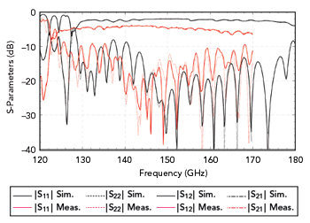
Figure 9 Measured versus modeled results of the flippable D-Band transitions.
Figure 9 shows the results from the most challenging configuration of the proposed transition. The measurements are for the back-to-back transition test circuit. The waveguide assembly and all the sources of loss are taken into account. The simulation spans 120 to 180 GHz, but the ZC170 mmWave converters limit the measurements to 170 GHz.
The results are promising since the back-to-back transitions maintain better than 10 dB return loss from 130 to 170 GHz. Insertion loss flatness is also verified throughout the D-Band frequency range with only minor ripple. We believe this ripple is mainly due to the length of the back-to-back transition configuration.
The main discrepancy is related to the absolute value of the insertion loss. The measured result is 4 dB in the 140 to 150 GHz range versus 2 dB predicted by the simulations. This deviation becomes larger in the 160 to 170 GHz spectrum, where the measured insertion loss reaches 6 dB at the top edge of the operational frequency. Several factors contribute to the observed difference. From the manufacturing standpoint, inaccuracies and tolerances lead to an insertion loss penalty. However, the electrical properties of the materials will also contribute to the loss deviation. The simulations take these material-related loss mechanisms into account, but the absolute values depend on the electrical characteristics of the materials that have not been experimentally validated in the 170 GHz spectrum.
CONCLUSION
The proposed D-Band coplanar-to-waveguide transition answers several technical and industrial needs, providing high performance and design robustness to practical assembly manufacturing. The layout requires a single 0.005 in. standard thin-film alumina layer with CPW-to-SIW and SIW-to-rectangular waveguide transitions. The integrated launcher guarantees hermeticity without a back-short in all four configurations. The transition configurations described in this article accommodate different MMIC and waveguide port requirements and provide a solution for most practical cases. Simulations and sensitivity analyses have been validated by back-to-back measurements, confirming a fractional bandwidth of about 30 percent with a 10 dB return loss. The proposed transition exhibits an average loss of 1.5 dB, de-embedded from the measurement fixtures, which is compatible with alternative, more complicated or less cost-effective solutions. The operation across the 130 to 170 GHz frequency range of D-Band makes this structure suitable as interconnection between MMICs and waveguide networks or antennas in next-generation wireless communication equipment.
ACKNOWLEDGMENT
This research work was funded by the Italian National Operational Program for Research and Innovation 2014-2022 (CCI 2014IT16M2OP005) European Social Fund, Action I.1.
References
- B. Tezergil and E. Onur, “Wireless Backhaul in 5G and Beyond: Issues, Challenges and Opportunities,” IEEE Communications Surveys & Tutorials 24.4 2022, pp. 2579–2632. doi:10.1109/COMST.2022.3203578.
- M. G. L. Frecassetti, A. Mazzanti, J. F. Sevillano, D. del Río and V. Ermolov, “D-Band Transport Solution to 5G and Beyond 5G Cellular Networks,” European Conference on Networks and Communications (EuCNC), 2019, pp. 214–218, doi: 10.1109/EuCNC.2019.8802033.
- A. O. Watanabe, M. Ali, S. Y. B. Sayeed, R. R. Tummala and M. R. Pulugurtha, “A Review of 5G Front-End Systems Package Integration,” IEEE Transactions on Components, Packaging and Manufacturing Technology, 2021, pp. 118–133, issn: 2156-3985. doi: 10.1109/TCPMT.2020.3041412.
- R. Quaglia, V. Camarchia, M. Pirola, Electronics for Microwave Backhaul, Artech House, 2016.
- A. U. Zaman, V. Vassilev, P.-S. Kildal and H. Zirath, “Millimeter Wave E-Plane Transition From Waveguide to Microstrip Line With Large Substrate Size Related to MMIC Integration,” IEEE Microwave and Wireless Components Letters 26, 2016, pp. 481–483. issn: 1558–1764. doi: 10.1109/LMWC.2016.2574995.
- E. S. Li, G.-X. Tong and D. C. Niu, “Full W-band Waveguide-to-microstrip Transition With New E-plane Probe,” IEEE Microwave and Wireless Components Letters 23, 2013, pp. 4–6. issn: 1558-1764. doi: 10.1109/LMWC.2012.2235176.
- C. Wang, Y. Yao, J. Wang, X. Cheng, J. Yu and X. Chen, “A Wideband Contactless CPW to W -Band Waveguide Transition,” IEEE Microwave and Wireless Components Letters 29, 2019, pp. 706–709. issn: 1558-1764. doi: 10.1109/LMWC.2019.2945242.
- S. Jameson and E. Socher, “A Wide-Band CMOS to Waveguide Transition at mm-Wave Frequencies With Wire-Bonds,” IEEE Transactions on Microwave Theory and Techniques 63, 2015, pp. 2741–2750. issn: 1557-9670. doi: 10.1109/TMTT.2015.2461160.
- Y.-C. Leong and S. Weinreb, “Full Band Waveguide-to-microstrip Probe Transitions,” Vol. 4, Anaheim, Calif., U.S., IEEE, 1999, 1435–1438, isbn: 0-7803-5135-5. doi: 10.1109/MWSYM.1999.780219.
- Y. Ishikawa, K. Sakakibara, Y. Suzuki and N. Kikuma, “Millimeter-Wave Topside Waveguide-to-Microstrip Transition in Multilayer Substrate,” IEEE Microwave and Wireless Components Letters 28, 2018, pp. 380–382, issn: 1558–1764, doi: 10.1109/LMWC.2018.2812125.
- S. Moscato, M. Oldoni and S. C. Mejillones, “Substrate Integrated Waveguide Components on Alumina for E-band Applications,” Microwave Mediterranean Symposium, 2022, pp. 1–4. doi: 10.1109/MMS55062.2022.9825525.
- Y. Zhang, D. Zhao and P. Reynaert, “A Flip-Chip Packaging Design With Waveguide Output on Single-Layer Alumina Board for E-Band Applications,” IEEE Transactions on Microwave Theory and Techniques 64, 2016, pp. 1255–1264, issn: 1557–9670, doi: 10.1109/TMTT.2016.2536602.
- S. R. Zahran, S. Moscato, A. Fonte, M. Oldoni, A. A. Traversa, D. Tresoldi, P. Ferrari, G. Amendola and L. Boccia, “Flippable and Hermetic E-Band RWG to GCPW Transition With Substrate Embedded Back-short,” IEEE Transactions on Microwave Theory and Techniques 71.6, 2023, pp. 2582–2593, doi: 10.1109/TMTT.2022.3228619.

