

MODELING THE ADC
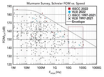
Figure 9 Walden FOM from Murmann survey.
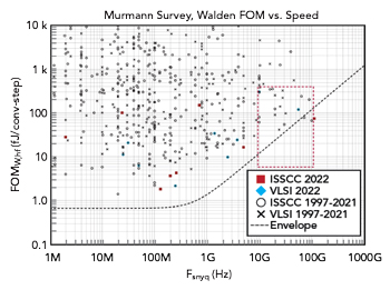
Figure 10 Schreier FOM from Murmann survey.
The ADC model uses behavioral equations derived from Murmann’s ADC survey population data.6 For a valid comparison, near-peer data points from similar-class ADCs are selected using two separate, but similar, FOMs. A black box ADC model allowing swept attributes is created from fitting population data points. The analysis uses two FOMs from the Murmann survey. The Walden FOM (FOMW) shown in Figure 9 favors low-resolution ADCs as it moves 2x per bit. FOMW is calculated in Equation 5 and a lower value is better.

The Schreier FOM (FOMS) shown in Figure 10 favors high-resolution ADCs as they move 4x per bit. FOMS is calculated in Equation 6, and a higher value is better.

As an important rule of thumb, DC power is proportional to the sample rate and exponential with dynamic range for a fixed FOM value.
The points in Figures 9 and 10 represent ADC conference presentations. The dotted “Envelope” line in the charts represents the expectation of commercially available future performance. The most successful ADCs balance dynamic range, sampling rate and DC power requirements.
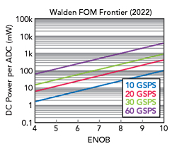
Figure 11 DC power vs. ENOB on the Walden envelope.
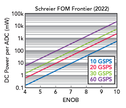
Figure 12 DC power vs. ENOB on the Schreier envelope.
Rearranging the FOM equations results in Equation 7. This data is plotted as DC power versus ENOB for the Walden FOM in Figure 11 and the Schreier FOM in Figure 12. These charts show how to trade off power and ENOB to arrive at the same FOM.

The attractiveness of a high speed ADC in an application involves a trade-off of ENOB, ISBW and DC power. Simultaneously excelling in all is very difficult. For example, a maximum DC power limit of 100 mW per ADC requires a compromise in sampling rate and ENOB for the application. At 60 GSPS, a state-of-the-art ADC will be ENOB=6. Lowering the sampling rate to 10 GSPS increases the ADC dynamic range to ENOB=8.7. Both ADCs are considered state-of-the-art, but the best solution depends on system priorities.
High sampling rate converters offer benefits in areas like frequency planning, instantaneous coverage, software-defined digital tuning and RF simplification. To fully understand the implications, designers must also understand DC power consumption and ENOB. The dynamic range, sampling rate and DC power consumption “triangle” determine overall ADC merit. In a radar application, for example, 60 GSPS at ENOB=6 might not be a better solution than 10 GSPS at ENOB=8.7. A high sampling rate might look attractive, but ENOB and power limit are often higher system priorities.
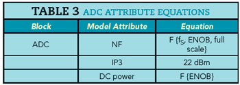
The ADC performance cascade model uses an RF black box with attributes NF, IP3 and DC power as shown in Table 3. These ADC attributes change as the system model sweeps.
The ADC NF is a function of ENOB or SNR as shown in Equation 8:
Noise spectral density, kTe (dBm/Hz), is equivalent to sensitivity (dBm) in a 1 Hz bandwidth. A 1 Hz bandwidth is assumed throughout, but this can be adjusted by adding a 10LogBW term. While this analysis focuses on noise, ADC two-tone IP3 performance is also important.
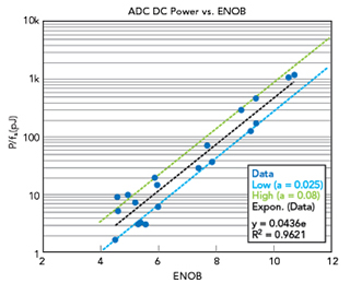
Figure 13 ADC DC power vs. ENOB.
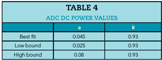
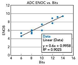
Figure 14 ENOB vs. bits.
The ADC DC power model uses data summarized in the Murmann survey. Figure 13 reduces the Murmann ADC survey data (rev20220719) to 20 members and filters for Analog Devices and industry peers, CMOS < 32 nm and fS>=4 GSPS to show the data and extrapolation of DC power as a function of ENOB. The curves in Figure 13 come from substituting the values of Table 4 into Equation 9.

Using the selected set of Murmann data, the model derives a relation for ENOB as a function of bits as shown in Equation 10 and plotted in Figure 14.

These equations describe a DC power and RF attribute model for the ADC as a function of ENOB. This is shown in Figure 15. Figure 16 shows DC power/channel versus ENOB in a system using digital beamforming.
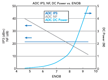
Figure 15 ADC NF, DC power and ENOB.
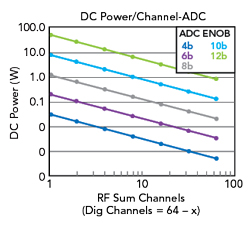
Figure 16 Beamforming trade-offs.
MODELING THE DIGITAL PAYLOAD
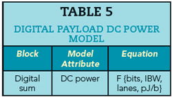
Table 5 Naval ships at the ready.
The high speed data payload and sum computation DC power are estimated from the transport energy per bit.6 The digital payload transport power associated with the ADC-to-digital sum node scales up as the number of digital sum channels and IBW increases. Table 5 shows the digital sum model attributes and Equation 11 calculates the high speed interface physical link transport DC power.

Equation 12 assumes a JESD link:
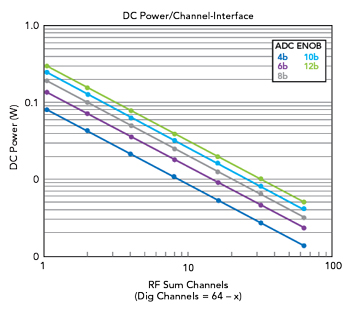
Figure 17 DC power response.
Figure 17 plots the DC power/channel including the interface versus summed RF channels for various ADCs.
CONCLUSION
Every phased array system has different beam attributes, sensitivity and dynamic range requirements for given DC power limits. A continuum of performance versus DC power solutions exists, but the best solution depends on the mission requirements. This article constructs an RF cascade model for a phased array receiver that analyzes the impact of RF and digital channel summation on dynamic range and DC power. The Excel model includes:
- RFFE
- RF channel summation
- ADC
- High speed digital interface and compute
- Digital channel summation.
Part 2 will present and analyze model results, relate the results to system FOMs and draw conclusions.
References
- T. H., Salvador, K.W. O’Haver, T. M. Comberiate, M. D. Sharp and O. F. Somerlock, “Benefits of Digital Phased Array Radars.” Proceedings of the IEEE, Vol. 104, No. 3, February 2016.
- W. F. Egan, “Practical RF System Design,” John Wiley & Sons.
- B. Annino, “SFDR Considerations in Multi-Octave Wideband Digital Receivers.” Analog Dialogue, Vol. 55, No.1, January 2021.
- P. Delos, S. Ringwood and M. Jones,“ Hybrid Beamforming Receiver Dynamic Range Theory to Practice,” Analog Devices, Inc., November 2022.
- www.analog.com/en/technical-articles/hybrid-beamforming-receiver-dynamic-range.html.
- B. Murmann, “ADC Performance Survey 1997–2022,” GitHub, Inc., 2023.