
Editor's Note: The author has revised this article. The new revision can be found here.
Many papers discuss the system trade-offs and relative merits of digital, analog and hybrid beamforming.1 Building on prior work, this article uses RF-to-analog-to-digital converter (ADC) cascade modeling to show dynamic range (linearity and noise) and sample rate trade-offs against DC power consumption in a multichannel system with varying channel summation in both the RF and digital realms. The optimal selection of sample rate, ADC effective number of bits (ENOB) and RF versus digital channel combining are weighed against DC power consumption. The Schreier and Walden ADC figures of merit (FOMs) are proposed as extensible to a multichannel system to express a single system FOM portraying optimal dynamic range normalized for DC power. Part 2 of this article will analyze the results and draw conclusions from system FOMs.
SYSTEM MODEL INTRODUCTION
In the phased array radar community, full digital beamforming gets a lot of attention. Significant government funding is leading to this capability rapidly evolving and the technique is an industry research hotbed. The promise of omnidirectional arrays with digital beamforming creating simultaneous beams enables software-defined multimission apertures and one array fits many missions. The appeal is multiple independent, simultaneous, software-configurable digital beams that improve detection and enable multifunction.1
In practice, there are multiple challenges to overcome; the biggest being DC power consumption. In elemental digital beamforming, the digitizer node (DAC/ADC) is distributed behind each element and must be of lower DC power than alternatives without sacrificing performance. Digitizer power is a function of dynamic range capability and sampling rate. Choosing the optimal ADC bit resolution and sampling rate, while being cognizant of RF performance, power consumption and digital versus analog beamforming capability is a complicated multidimensional puzzle for phased array system designers.
Thermal limits and size are also factors. Larger phased arrays often employ blades that put the electronics orthogonal to the antenna face, offering thermal and size flexibility. Some systems, especially those at higher frequencies, require electronics that are planar with the antenna and fit within the element lattice spacing. This creates challenging thermal and size problems. The electronics must get smaller and shed power without sacrificing performance.
SYSTEM FIGURES OF MERIT
Dynamic range, or spurious-free dynamic range (SFDR), is the most common receiver FOM and is a function of linearity and sensitivity. Receiver SFDR is different than ADC SFDR. ADC SFDR quantifies the maximum ADC spur among harmonics, interleaving spurs, clock leakage and intermodulation products and is not a direct representation of two-tone linearity. Receiver sensitivity is the minimum detectable signal level at some offset threshold from the noise floor. Considerations like waveform type and probability of detection determine the offset threshold, which is set to zero in this paper. Sensitivity does not consider linearity; it is solely a noise metric. A point of emphasis: radar and electronic warfare (EW) systems operate in blocker environments, so linearity (two-tone intermodulation) is as important as noise. Phased array systems are generally sub-octave and IMD3 distortion is most important. Conversely, EW systems are multi-octave and IMD2 and IMD3 distortion is most important. A radar or EW receiver is typically not optimized only for sensitivity. Linearity is an important design goal and receiver SFDR is a handy FOM because it considers both sensitivity and linearity. Figure 1 illustrates the noise contribution from various processes and components.

Figure 1 Noise contribution of ADC SNDR, NF, IFBW, IMD3 and SFDR.3
SFDR is a single-point FOM that expresses the best-case SNR and distortion at a singular best-case RF input power. This occurs when the IMD spurs are at the same level as the noise.2 SFDR can be expressed as shown in Equation 1:

Where the processing bandwidth of the noise channel (IFBW), often set using a combination of IF and digital filtering and the thermal noise spectral density, is ‐174 dBm/Hz at T=290 K.
The model analyzes SFDR and sensitivity system performance FOMs. These metrics are processing bandwidth dependent and the processing bandwidth is set to IFBW=1 Hz. To adjust for the specific processing bandwidth:
- Add 10log(IFBW) to the sensitivity
- Subtract (2/3 x 10log(IFBW)) from SFDR
A receiver often has simultaneous sensitivity and SFDR requirements. Low RF front-end (RFFE) noise figure (NF) helps IP3 and SFDR, but gain helps sensitivity and hurts SFDR. A “Goldilocks” RFFE has enough gain to meet sensitivity requirements but not too much for fear of degrading SFDR. As a rule of thumb; never design a receiver with excess gain.
SYSTEM CASCADE MODEL
The objective is to build a simple Excel model that accommodates swept RF, digital beamforming ratios, ADC ENOB and DC power consumption derived from Murmann survey data. This data will be used to determine the best performance/DC power consumption solution. The cascade model includes the RFFE, channel summation, ADC and digital channel summation. Figure 2 shows the modeled blocks and cascade metrics at each node. The model uses the method for summed RF channel cascade analysis described by Delos et al.4 The key to the model is to track device-additive and cumulative noise spectral density, kTe, at each node and account for signal gain and noise gain separately.
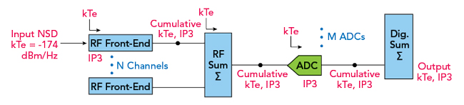
Figure 2 Phased array cascade model using analog and digital beamforming and summation.
Using this model, it is possible to get a negative system NF with summed RF channels, which is exactly the desired advantage of coherent summation as shown in Equation 2:

Where F (noise factor)=SNRinput/SNRoutput
NSD = noise spectral density.
The examples use a 64-channel subarray. When plots show channel summation, the horizontal axis ranges from 64-channel digital at the origin to 64-channel RF on the right of the axis, with a blend in between. The blend is called hybrid beamforming with increasing RF sum from left to right. ADC ENOB is swept in the analysis and presented in the plots. Trends in DC power and performance are analyzed as these parameters are swept.
MODELING THE RFFE
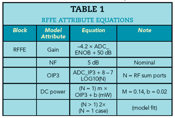
The RFFE model is an RF black box with gain, NF, IP3 and DC power that are functions of swept attributes. As the system model sweeps the RF, digital sum ratio and ADC ENOB, the RFFE attributes tune for the best cascade performance. Table 1 provides the attribute function equations.
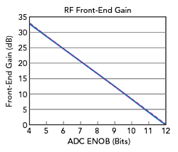
Figure 3 RFFE gain vs. ADC_ENOB.
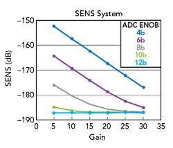
Figure 4 Overall sensitivity vs. RFFE gain for varying ENOB.
The model sets RFFE gain as a function of ADC_ENOB, a swept parameter, as shown in Figure 3. The model uses a linear equation to set a minimum viable gain for reasonable system kTe while seeking to maximize SFDR. RF gain reduces SFDR, so it should be minimized to just meet NF requirements. Lower-resolution ADCs have a much higher NF and require more RF gain to set acceptable system NF. In contrast, an ADC with ENOB=12 has excellent NF and requires no front-end gain. This provides a big dynamic range benefit, albeit at an ADC DC power penalty. The effect of sensitivity from RFFE gain and ADC ENOB is shown in Figure 4. Figure 5 shows the gain impact on SFDR for an ADC with ENOB=8 and Figure 6 shows the same analysis for an ADC with ENOB=12. The ENOB=8 case sees improving sensitivity and neutral SFDR impact as the gain is increased to approximately 15 dB. Above 15 dB, SFDR begins to degrade. In contrast, the ENOB=12 case has superior ADC NF, requiring no gain in front. Putting the same 15 dB gain block in front would have a net negative impact on ENOB=12 performance.
Figure 5 RFFE gain impact on SFDR for ADC ENOB=8.

Figure 6 RFFE gain impact on SFDR for ADC ENOB=12.
For these simulations, the RFFE block is set to NF=5 dB and OIP3=30 to 40 dBm. These values are realistic and acknowledge the linearity trade-off. These simulations also assume RFFE filtering, switching, limiting and other loss elements.
The model sets RFFE OIP3 as a function of ADC_IP3 and the number of summed RF ports. The result where every element uses digital beamforming and ADC IP3=22 dBm is shown in Figure 7. This shows that a single port requires an RFFE OIP3 of 30 dB, 8 dB higher than the ADC IP3, for a degradation to system-cascaded IP3 of approximately 0.8 dB. Summing up more RF channels eases the single-channel OIP3 requirement, which eases the RFFE DC power requirement.
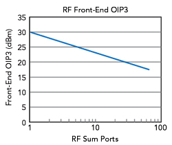
Figure 7 RFFE OIP3 vs. the number of summed RF ports.
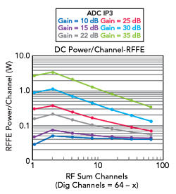
Figure 8 RFFE DC power/channel.
DC power is an important consideration and the model sets RFFE DC power as a function of RFFE OIP3, which is a function of ADC IP3 and RF sum ports. For the case of RF=1, the RFFE is a variable gain stage with signal filtering. The RF > 1 case sums more than one RF path and the RFFE architecture requires time or phase delay and attenuation control for beamforming. The model assumes a time delay unit (TDU) and a variable attenuator (DATT) between two gain stages. The extra gain stage doubles the DC power, but it is required to overcome the TDU and DATT loss. The results of the analysis are shown in Figure 8, where the doubling of DC power is evident. Figure 8 also shows increasing RFFE DC power with increasing ADC IP3.
MODELING RF CHANNEL SUMMATION
RFFE single-channel OIP3 decreases with increasing RF channel summation. Summing RF channels improves SNR by coherently adding the signal and noncoherent Gaussian white noise. Improved SNR is an advantage, but this creates a larger signal before the nonlinear ADC than digitally summing channels after the ADC. The spur level resulting from multitone intermodulation is a function of ADC IP3 and the signal level into the ADC. For two tones at the same level, Equation 3 specifies:
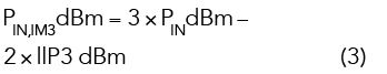
Summing before the ADC improves SNR but degrades the two-tone spurs due to ADC nonlinearity compared to the same N channels summed digitally after the ADC. The SFDR improves by digitally summing and computing the gain after the ADC. The ADC handles a lower signal and the SNR benefit is realized through the combination of digital data streams at the price of bit growth.
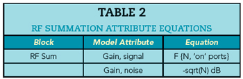
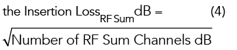
To understand the effects of summing channels, we use a method of passive RF summation developed by Analog Devices.5 With passive summation, there is insertion loss but no additive noise and no impact on IP3. RF summation benefits SNR and has no impact on IP3 because intermodulation spurs add coherently across combined channels, like the signal. Because of RF combiner loss, the sensitivity degrades as the summed channels increase. This is modeled in Equation 4 as:
The RF sum attributes are shown in Table 2.