

A secure communication system with a spectrum scanning feature is realized with a programmable system-on-chip (PSoC) embedded system platform. The development of this complex electronic system is possible due to the fast data processing and internal signal processing capabilities provided by PSoC controllers. This PSoC-based communication system can operate in an environment with intense channel noise and external disrupting RF signals through the transmission of data packets from different channels whose frequencies change dynamically with time. It enables emergency communication with specialized hardware and a unique algorithm.
When exposed to electromagnetic disturbance, the communication between a transmitter and receiver is interrupted. When a jamming signal is present, a certain region of the electromagnetic spectrum becomes unusable. An emergency communication system is needed when systems such as radio, mobile phone, GPRS, M2M, Bluetooth, Wi-Fi, industrial, scientific and medical (ISM) RF modules and satellite connections, which are today’s primary communication tools operating in the UHF band, become unusable due to noise.1
The system should incorporate automatic channel scanning, frequency hopping and channel listening with received signal strength indicator (RSSI) information distinguishing between noise and data to provide multi-channel broadcasting and reception. This article describes a secure wireless communication system that can perform automatic channel scanning and channel synchronization to create new communication channels under the influence of electromagnetic noise and interference. It is accomplished with a programmable system platform on a chip.
Several commercial RF receiver, RF transmitter and RF receiver/transmitter modules are examined. The HopeRF RFM22B transceiver module was selected due to its channel selection, frequency hopping, RSSI feedback and multi-channel RF communication capabilities.
The features that enable the design, however, are the algorithm and the capabilities of the embedded system platform. There are several platforms available, including Raspberry Pi,2 Zynq,3 Jetson,4 Altera Cyclone II,5 Beagle Bone,6 Odroid,7 STM328 and Cypress PSoC.9 In this study, the Cypress PSoC is used because it has a CPU core and configurable analog and digital blocks that differentiate it from traditional microcontrollers. The Cypress PSoC provides ease of use to the designer in the algorithm’s implementation, development and debugging phases.
In this design, there is a primary circuit that provides the data to be sent, a secondary circuit that receives the sent data and a noise generator to test the performance of the communication system in the presence of interference. The noise generator acts as a jammer that broadcasts on the desired channel. The primary device ensures that the data entered from the keyboard is transmitted on an empty channel that does not contain noise. The secondary device captures the data synchronously to the channel where the primary device is tuned. Notification that the data has been received is also sent to the primary device. The associated algorithm ensures that the data is transmitted in a safe and secure manner.10-13
SYSTEM DESCRIPTION
The RFM22B is a low-cost wireless ISM transceiver module operating in the 240 to 960 MHz range. It consumes 55.5 mW of power in receive mode and 265 mW at maximum output power in the transmit mode. RFM22B communication modules have -121 dBm receive sensitivity and +20 dBm maximum output power. They can provide communication up to very long distances in open space, considering the free space path loss at the operating frequency.
Antenna diversity and frequency hopping support can be used to extend the range and improve performance. Additional system features such as an automatic wake-up timer, low battery detector, 64-byte Tx/Rx-FIFO, automatic packet processing and preamble detection reduce overall power consumption and enable the use of low-cost system MCUs.14
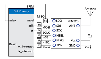
Figure 1 SPI connections of RFM22B in the PSoC Creator program.
The Cypress PSoC comprises a CPU core and configurable analog and digital blocks that differentiate it from traditional microcontrollers. The PSoC and RFM22B modules communicate using the serial peripheral interface (SPI) protocol. SPI connections are shown in Figure 1. The RFM22B receives data from the PSoC through the SCLK, SDI and nSEL pins. The PSoC reads data from the RFM22B transceiver’s SDO output pin. PSoC Creator software from Cypress enables the generation of programs for the PSoC 5LP system-on-chip.
The communication protocol is used to write to or read from the registers on the integrated PSoC. The SPI data exchange is as follows:
The 1-bit read-write select bit (R/W) takes place as a 16-bit string, with the following 7 bits of address space and the last 8 bits of data. Here, if the read-write select bit is zero, reading from the 7-bit address is performed, and if it is one, writing to the 7-bit address is performed.
After writing to the desired address, the SS pin drops to zero, the R/W bit is set to one and the desired address is sent in the following 7 bits. The 8-bit data following the address is written to the desired address in this way. Writing is accomplished by transferring a bit on the rising edge of the clock signal.
In the SPI protocol, the SS pin must first drop to zero for data exchange to start, and the secondary must be selected in this way. No data exchange is possible without selecting a secondary. In the read operation, the R/W bit is set to zero and the address is sent in the following 7 bits. The 8-bit data that follows the address is set to zero and filled with the data read from that address. This operation is performed on the rising edge of the clock signal, as in the write operation.
The RFM22B is programmed using the SPI protocol, allowing the use of frequency shift keying (FSK),15 Gaussian frequency shift keying (GFSK)16 and on/off keying (OOK)17 modulation types.
Primary and Secondary Circuit Designs
The embedded system design uses the PSoC 5LP system-on-chip (see Figure 2). In the primary circuit, there is a keyboard for data input, a 2x16 LCD user interface screen, an RFM22B transceiver module and an antenna unit to generate multi-channel RF signals. In the secondary circuit, the use of a keyboard is optional; for one-way communication, there is no need for a keyboard.
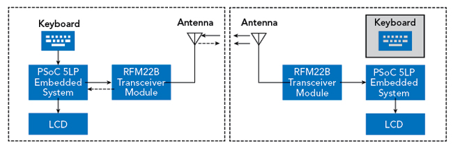
Figure 2 Primary and secondary circuit block diagrams.
In the primary circuit, a mini keyboard (cardKB), employing the I2C serial communication protocol, is used to enter data into the system. With dimensions of just 84 × 54 mm, it has 50 keys, 1 neopixel LED, an Atmega328P processor and a communication port. Different characters can be sent using the shift, ctrl, alt, sym and fn keys.
Figure 3 is the corresponding schematic of the primary and secondary circuits with a CY8C5868AXI-LP035 model PSoC. The PSoC is packaged in a 100-pin thin quad flat pack clocked by a 24 MHz crystal. Serial wire debug programming outputs are used to facilitate programming operations.

Figure 3 Primary/secondary circuit diagram.
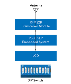
Figure 4 Noise generator circuit block diagram.
A noise generator circuit enables external parameter adjustment and functions as a jammer for testing as well (see Figure 4). The miniature switch (DIP switch) in the noise generator circuit is used to select the frequency band for noise injection.
The communication system printed circuit boards (PCBs) are shown in Figure 5. The primary and secondary circuit PCBs are in red and the black PCB is the multi-channel RF noise injection circuit.
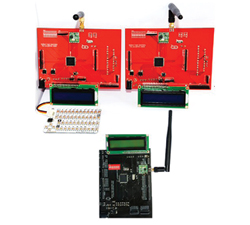
Figure 5 Communication system fabricated PCB assemblies.
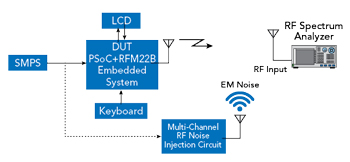
Figure 6 Test circuit block diagram.
EXPERIMENTAL RESULTS
The setup of Figure 6 is used for system evaluation.
Scenario-1: Transmission of Data Packets from Different Channels in the Presence of Noise
In the first scenario, the dynamic behavior of the system is examined with noise injected in different channels during transmission of the sample message “DATATEST” consisting of eight letters. Each letter of the word “DATATEST” is transmitted at 1-second intervals and there is no noise signal in the environment when the system is energized.