
Equation (5) describes the capacitance value C2f0 of the output terminal at the second harmonic. Note that the fundamental and second harmonic impedance traces should have opposite directions.28
To determine the optimum load impedance at high power, the loads are modified through large-signal harmonic balance simulations for the third stage transistor nonlinear output capacitance, which affects the capacitance value C2f0.
Output matching is a two-stage L-type low-pass network to expand the bandwidth, shown within the blue dotted line in Figure 3a. The minimum Q of the OMN is expressed in Equation (6), where Rload is 50 Ω.

It can be seen in Equation (7) that the series LC tank, (Ctrap and Ltrap) for the third harmonic (3f0) trap creates a short-circuit load at 3f0.

Figure 3b shows the load impedance trajectories. The fundamental theoretical impedance (Ropt) of the OMN is shown in red. The second harmonic impedances from 10 to 14 GHz are nearly 1.178 x Ropt. The third and higher-order harmonic impedances at the load plane are also terminated to short circuits. The optimum fundamental and second harmonic impedance design approach controls the bandwidth with a low Q OMN and by determining the impedance transformation, independently.
PA FABRICATION AND PERFORMANCE
Figure 4 is a microphotograph of the PA with a chip size of 1.8 × 0.8 mm. The total quiescent current is approximately 132 mA with a supply voltage of 5 V and a bias voltage of 2.9 V. RF input and output pads are bonded using 25 µm diameter gold bond wires to 50 Ω microstrip. Power supply pads are wire-bonded to the printed circuit board traces.
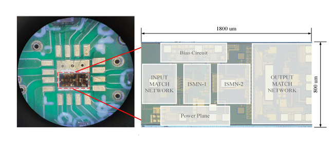
Figure 4 PA microphotograph.
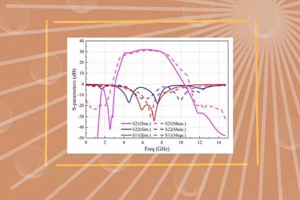
With a continuous wave input signal, the experimental results are shown in Figures 5 through 9. Simulated and measured scattering parameters of the PA are shown in Figure 5. It achieves a small-signal gain of 30 and 31.5 dB, input return loss of 15 and 35 dB and an output return loss of 5 and 18.5 dB at 5 and 7 GHz, respectively. Measured S-parameters agree well with the simulation. Differences are attributed to inaccurate bond wire modeling, board parasitics and crosstalk due to the board layout.
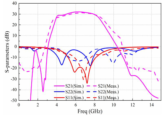
Figure 5 PA S-parameters from 0 Hz to 15 GHz.
Maximum output power over the band is between 29.5 and 30 dBm, while power-added efficiency (PAE) is between 36 and 42.7 percent (see Figure 6).
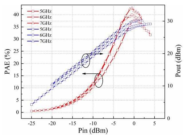
Figure 6 Measured output power and PAE vs. input power at frequencies across the band.
Simulated and measured AM-to-AM and AM-to-PM conversion at 6 GHz are plotted in Figure 7a. The PA exhibits a measured AM-to-AM conversion of 29.5 dB on average with 0.5 dB variation from 0 to 30 dBm input power. The variation of AM-to-PM in the fabricated PA is 1 to 5 degrees. For a 1024 QAM modulation signal, Pout meeting an error vector magnitude (EVM) of –40 dB is 16.7, 18.2, 20.6, 19.5 and 17.8 dBm at 5.0, 5.5, 6.0, 6.5 and 7.0 GHz (see Figure 7b).
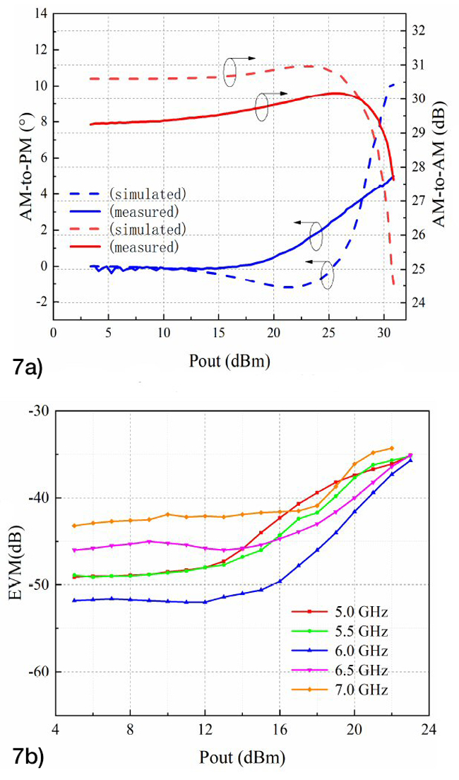
Figure 7 AM-to-AM and AM-to-PM as a function of output power at 6 GHz (a) and EVM as a function of output power at different frequency points (b).
Figure 8 shows the measured saturated output power (Psat) and output 1 dB compression point (OP1dB) from 4.4 to 7.6 GHz, while Figure 9 shows the measured second and higher-order harmonic suppression with an output power of 27 dBm at 6 GHz.
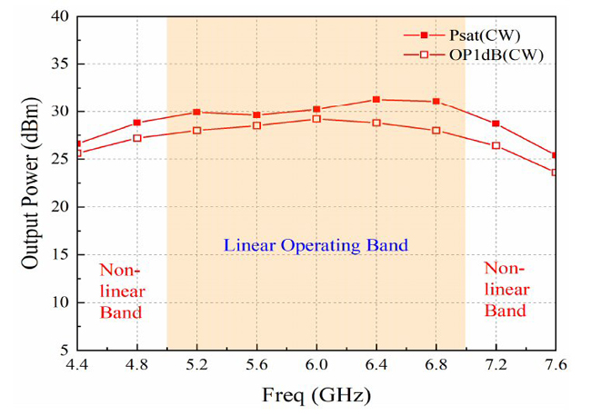
Figure 8 Measured Psat and OP1dB from 4.4 to 7.6 GHz.
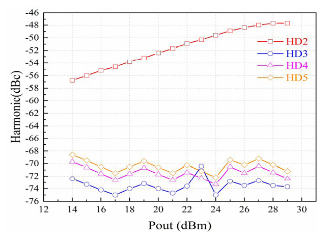
Figure 9 Measured second and higher-order harmonic suppression at 6 GHz.