
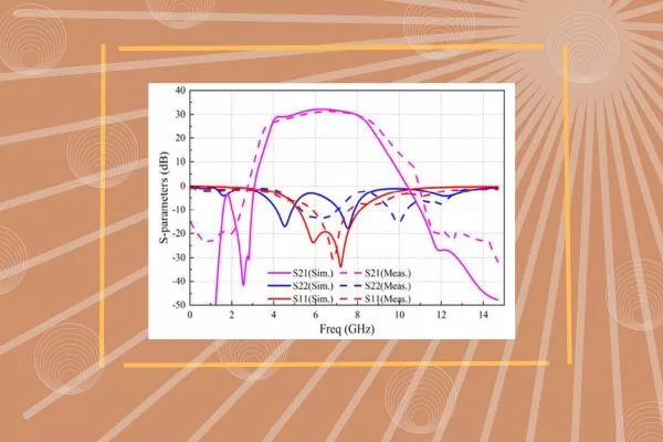
A broadband power amplifier (PA) with a small chip size of 1.8 x 0.8 mm2 based on GaAs heterojunction bipolar transistor (HBT) technology is designed for C-Band. By setting the optimal load impedances in accordance with Class-J mode operation and incorporating a low Q output matching network, high efficiency is achieved. With a 5 V power supply and 2.9 V bias, a 3-stage PA demonstrates 30 ± 0.5 dB of small-signal gain and greater than 29.5 dBm of saturated output power with 36 percent power-added efficiency over its operating band from 5 to 7 GHz at room temperature.
One of the main challenges facing current satellite communication technology is power consumption, which impacts reliability and the efficient use of spectrum.1,2 Another major challenge is bandwidth. For a multi-band wireless communication system, wideband amplifier characteristics can enable more frequency bands with less hardware. In this context, broadband communication systems amplifiers came into being and have been widely applied in modern commercial systems.3-5
A single broadband high efficiency PA can provide savings in material costs, weight and power consumption. This is especially important for satellite communication at C-Band for operation during natural disasters, where C-Band frequencies provide more reliable connections.6,7 In addition, C-Band is useful for Wi-Fi devices and radar systems.
Linear, broadband and high efficiency power amplifiers are, therefore, key components of RF front-ends.8 For traditional wide bandwidth PAs, there is a tradeoff between efficiency and linearity. Generally, high efficiency is achieved by changing the static bias point to reduce the conduction angle and linearity is improved by suppressing higher harmonics.
To address this tradeoff, a second harmonic tuned high efficiency PA mode is employed.9-15 Recently, a newly developed Class-J mode of operation has demonstrated its potential for high efficiency and wide bandwidth applications while maintaining linearity.16-18 The new approach provides the same efficiency as conventional Class-AB PAs and addresses high second harmonic currents for improved linearity.
CLASS-J POWER AMPLIFIER AND MATCHING METHOD
In wireless communications, the traditional technique for achieving high efficiency power amplifiers is to operate in deep Class-AB mode.19-21 Fourier series analysis of the Class-AB power amplifier waveform shows that it has a high second harmonic current level.22
To obtain a sinusoidal collector voltage waveform at the fundamental frequency of an HBT, deep Class-AB operation requires a resistive load at the fundamental frequency and a short-circuit termination for all harmonics, which also affects the output power and reduces efficiency. In a practical design, the second harmonic shorting terminal is accomplished by using a trap at the collector of the output transistor operating at the second harmonic frequency.23-26
The wave trap is a parallel branch composed of a capacitor and an inductor in series to achieve resonance at the second harmonic. Due to the influence of operating frequency and circuit parasitic parameters, the second harmonic termination tends to become capacitive. Therefore, the main factor affecting efficiency is the deviation of the harmonic termination. In addition, shorting the second harmonic requires a high Q trap, which is contradictory for wide bandwidth.
Thus, to achieve a wide bandwidth with maximum efficiency, the PA design must leverage the second harmonic, while avoiding direct use of a second harmonic resonant circuit. The method used in such a design is the Class-J mode PA.
Class-J PA Design
A simplified schematic of the three-stage PA is shown in Figure 1. The transistor sizes of the first, second and third stages are 200 µm2, 420 µm2 and 2,600 µm2, respectively. The passive components have the following values: C1 = 3 pF, R1 = 400 Ω C2 = 2 pF, C3 = 3 pF, L1 = 0.5 nH, C4 = 1.6 pF, R2 = 2000 Ω C5= 1pF, C6 = 2 pF, L2 = 0.05 nH, C7 = 8 pF, C2f0 = 3.2 pF, Ctrap = 0.34 pf, Ltrap = 0.23 nH, L4 = 0.15 nH, C8 = 0.6 pF, L5 = 0.18 nH and C9 = 0.63 pF.
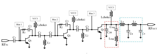
Figure 1 Three-stage PA schematic.
The first stage is biased in Class A mode for the highest linearity. The second stage operates in shallow Class-AB mode for higher linearity and better efficiency. The third (output) stage operates in Class-J mode for bandwidth extension and linearity enhancement.
To realize better flat gain and linearity, AM-to-AM and AM-to-PM flatness characteristics are important. The output stage operating with low quiescent current bias and Class-J output matching exhibits gain expansion and lagging phase shift characteristics. To compensate for these nonlinearities, the second stage is designed to have gain compression and leading phase shift characteristics, and the first stage is optimized to deliver flat gain and phase shift. Hence, the PA achieves flat AM-to-AM and AM-to-PM performance over a wide range of output powers (see Figure 2).
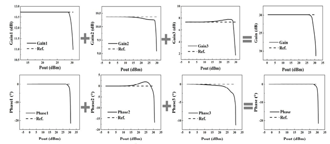
Figure 2 Three-stage linear amplifier design stage gain and phase considerations.
Class-J Mode of Operation
Proper output matching network (OMN) design is essential for optimum PA performance. The Class-J load for the maximum fundamental voltage component is determined from the optimal Class-B fundamental load.27 Figure 3 shows the OMN circuit and its characteristic, where a parallel capacitor is added at the collector of the output transistor so that the output voltage waveform is 45 degrees different from the original voltage waveform.
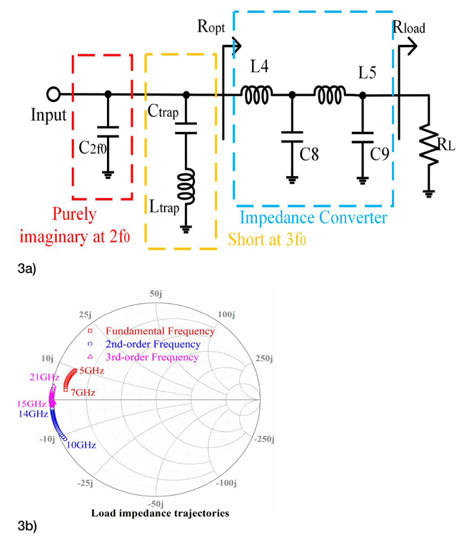
Figure 3 OMN (a) and load impedance trajectories (b) for the Class-J mode.
The expressions for the current and voltage waveforms are:
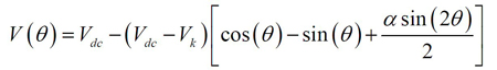
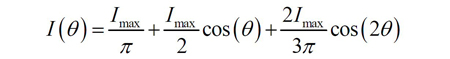
Where θ is the conduction angle.
Equations (3) and (4) represent the fundamental impedance ZL1 and the second harmonic impedance ZL2, respectively.
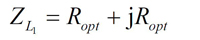
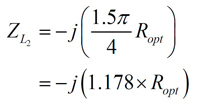
Where Ropt is the optimal load impedance with a small fundamental wave at the maximum current.