
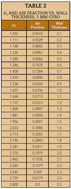
More modern and sophisticated AM dielectric foam is fabricated using more complex lattices based on a unit cell design, such as a gyroid for a gradient-index of refraction (GRIN) lens (see Figure 2). This approach enables the unit cell to be designed with a given air-to-dielectric volume fraction (see Figure 3 and Table 2), and for larger structures to be developed from a 3D matrix of unit cells. Hence, very precise control of the volume fraction can be achieved and the design of a 3D object larger than a unit cell is a relatively simple matter of filling a volume with unit cells and potentially even partial unit cells that still meet the volume fraction criteria.
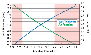
Figure 3 Gyroid effective permittivity and air fraction vs. wall thickness.
Combining unit cells and varying the unit cell volume fraction can be used to realize variable dielectric performance, effectively realizing metamaterial dielectric structures. With proper design, this technique can be used to design and fabricate 3D RF lenses, such as GRIN Luneburg-style RF lenses.3-5 There are a variety of other uses for metamaterial dielectric structures made from AM materials, however, to achieve air-like or dielectric foam-like performance, the volume fraction of the lattice structure must be as conformal throughout the volume as possible.
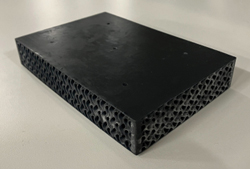
Figure 4 3D printed foam material.
Unlike dielectric foams, air-like AM dielectric foam can be designed so that the external surfaces that undergo stress are solid or incorporate additional structures that are more wear resistant, have higher compressive strengths (up to 400 PSI currently), or can be designed to better support attachments or fixturing. In fact, an AM dielectric foam can be designed in such a way that all mechanical and structural features are fabricated along with the air-like volume sections (see Figure 4). With this capability, indexing structures and mechanical attachment points can be manufactured in a single step, as opposed to various steps with the potential for tolerance and yield issues.
Using an AAS as an example, an air-like AM dielectric foam can be designed such that the coupled antenna structures are precision indexed from the top and bottom sections of a laminated stack with the air-like volume sections in between the coupled antennas and denser sections toward where the indexing, attachment and/or fixturing points are located. In this way, the surfaces to be laminated, metallized or otherwise combined with the AAS stack can be designed to reliably withstand the forces intrinsic to lamination or other manufacturing/assembly stages.
RF lenses and/or radomes can also be fabricated using AM technologies that enhance the coupled antenna structure performance using the same technology, which may potentially limit sourcing and supply chain issues of the RF dielectrics and reduce AAS bill-of-material complexity.
Using an AM dielectric foam approach to design and fabricate AASs or similar complex RF structures fundamentally changes the design approach and can possibly simplify the design by enhancing the degrees of freedom available to designers.
One area of simplification is in the design process, through electromagnetic (EM) simulation, parametric optimization and iterative design practices. Making use of AM dielectric foam, including air-like structures, enables very rapid prototype and development cycles, especially in software. Where traditional dielectric foam and other dielectric structural materials must be mostly designed in advance and only tweaked slightly based on feedback from EM simulation and parametric optimization, an AM-EDS approach allows for much more freedom of design and simulation with proxy structures that can then later be refined and fabricated with AM dielectric foam. This includes non-planar structures and even larger structures, as indexing can be designed into AM dielectric foam parts.
POTENTIAL OF AM DIELECTRIC FOAM
One of the largest drawbacks of dielectric foams is that they are not readily metallized without lamination or some other type of adhesive attachment of metallic conductors. There also is no clear path toward metallizing dielectric foams to produce conformal and planar metallic layers suitable for RF transmission lines and circuits.
This includes creating metallic vias in the z-axis. It is possible to insert a cylindrical metallic conductor tubes or pins inside a machined hole in a dielectric foam and use some type of conductive adhesive or soldering process to form a via, though this process is somewhat error prone and not as high performing as true vias with metallic attachments, such as soldering or selective metallization. Inserting via tubes or pins may also lead to clearance issues with the top and bottom laminated sections in a stack.
This is one of the key areas where AM dielectric foam has the potential to address many of the design challenges associated with AAS and other high performance stacked RF circuits. It is already possible to perform reliable and high performance selective metallization or even complete metallization of AM-EDS materials that are well suited to very high frequency (greater than 90 GHz) applications. Using air-like AM dielectric foam with design features, such as a solid planar surface with good surface finish and solid-wall via sections, for selective metallization can enable truly 3D RF circuits with air-like dielectric structures and dielectric substrates in a simplified process.
There are clearly some limitations on the thickness and diameter of vias that can be metallized with selective metallization processes, such as laser selective activation metallization, though non-selective techniques using electroless metallic plating could enable even small and high aspect ratio vias to be developed if there is a method for masking of the portions of the structure that should not be metallized. Conical vias could also be viable for selective metallization of the inner wall of the via structure, which would enable laser selective activation in even high aspect ratio vias.
With more development in metallization processes and early involvement of AAS and RF designers in the design process, it may be possible to design entire AAS and complex RF structures using (AM) dielectric foam technology, including the dielectric substrates, planar/3D circuit elements including vias, air-like (low Dk and low Df) volumes, RF lenses, radomes, RF windows and even the structural elements. It is possible to AM both low Dk and low Df polymer composite, as well as low Df ceramics for high-power and high heat applications.
CONCLUSION
Air-like AM dielectric foam can be designed to support high pressure and precision lamination; and, it provides a pathway for selective metallization and metallic vias. The different materials available and the degrees of freedom enabled by AM of dielectrics provides designers with a much greater potential to innovate and work around previous challenges in the design process of complex 3D RF systems, such as AASs.
References
- S. Chenu, J. -P. Coupez, F. Karpus and B. Toublanc, “Development of New Technologies Using Foam Materials for RF Device Integration,” 43th European Microwave Conference, October 2013.
- S. Zhang, C. Njoku, W. Whittow and J. Vardaxoglou, “Novel 3D Printed Synthetic Dielectric Substrates,” Microwave and Optical Technology Letters, Vol. 57, No. 10, July 2015, pp. 2344–2346.
- “Applications Guide to 3D Printed Low-Loss Dielectric Structures Addressing Microwave/mmWave Challenges,” Fortify, Web: https://3dfortify.com/white_papers/applications-guide-to-3d-printed-low-loss-dielectric-structures-addressing-microwave-mmwave-challenges.
- “Ku-Band/Ka-Band Simulation & Testing of a 3D Printed Dielectric Lens Fabricated from Low-loss and Los-dk Resin,” Fortify, Web: https://3dfortify.com/case_studies/ku-band-ka-band-simulation-testing-of-a-3d-printed-dielectric-lens-fabricated-from-low-loss-and-los-dk-resin.
- Fortify, “3D Printed Dielectric Lenses Increase Antenna Gain and Widen Beam Scanning Angle,” Microwave Journal, White Paper, July 2021, Web: https://www.microwavejournal.com/articles/36375-d-printed-dielectric-lenses-increase-antenna-gain-and-widen-beam-scanning-angle.