
The purpose of this work is to point out some of the more subtle points of combline filter design. These issues vary depending on the technology used to realize the filter. While these issues may be well-known to practitioners of the same generation as the author, they may not be well understood by the current generation of engineers, students and academics. Our goal is to find simulation and design methods which fully predict the performance of the combline filter in both the passband and the stopbands. While the coupling matrix method is quite popular today, we will demonstrate how it fails to fully predict the performance of combline filters in several practical situations.
COMBLINE FILTERS
One of the most useful and flexible microwave filter topologies is the combline filter.1 We can realize these filters as high Qu cavity filters and as thin-film or printed circuit board planar filters. In the case of narrowband filters we can add cross-couplings that realize transmission zeros in the stopbands, which enhance selectivity. Millions of cross-coupled cavity combline filters and diplexers have been deployed around the world to support cellphone networks. Over the years a smaller number of high performance combline filters and multiplexers have also been designed for military and satellite applications.
THE COUPLING MATRIX
The basic concept of cross-coupled filters was demonstrated in the mid-1960s by Johnson2 and Kurzrok.3,4 The coupling matrix has become ubiquitous in the filter community since the seminal paper in 1972 by Atia and Williams.5 Today, many published filter papers include a coupling matrix. Most would agree that the basic coupling matrix concept represents a narrowband, lumped element filter approximation with frequency independent couplings.
It is generally agreed that coupling matrix synthesis should be valid up to about 10 percent relative bandwidth. Some researchers have attempted to enhance the coupling matrix by introducing frequency dependent couplings. One claimed advantage of the coupling matrix is that once the matrix is synthesized, many topologies can be generated, although most of those topologies have very high tuning sensitivity and are not very useful.
INLINE CAVITY COMBLINE FILTERS
In Figure 1 we find a 3D Finite Element Method (FEM) model of an N = 8 inline cavity combline filter. The resonators are typically 30 to 60 degrees long, depending on bandwidth. Capacitive loading brings them to resonance. Three styles of loading are typically used: resonator loading where the tuning screw penetrates the resonator open end, lumped loading with no screw penetration and cover loading where the resonator extends into a pocket in the filter cover. Tapping into the first and last resonators is the most common and flexible input/output scheme. Capacitive coupling with a probe or disk and inductive coupling with a grounded loop are also possibilities.
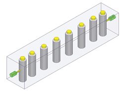
Figure 1 N = 8, 20 percent bandwidth inline combline filter with lumped loading, modeled in Ansys HFSS.
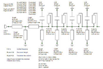
Figure 2 Partial schematic for the N = 8 combline filter, modeled in Cadence Microwave Office.
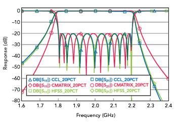
Figure 3 Comparing simulation from the circuit model (blue), HFSS model (green) and coupling matrix (red).
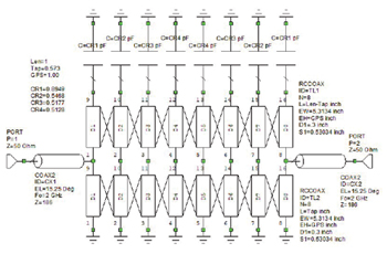
Figure 4 Simplified TEM model with the physical GPS = 1.00 in.
If we wanted to develop a design program6 for the inline combline filter, we could first synthesize a commensurate round rod array7 and modify the result to be equal diameter. Adding the tuning screw details can only be done through optimization. Adding the input and output taps also requires optimization.8 At this point, we have a set of dimensions and a network theory model of the filter (see Figure 2).
If we build hardware at this point or make a 3D FEM model of the filter, we find that the filter bandwidth is much larger than predicted. This is the well-known bandwidth expansion problem for inline cavity combline filters.9 Although the resonators are sitting in a waveguide below cutoff, they can generate evanescent modes in the cavity that modify the assumed transverse electromagnetic (TEM) coupling values.
We can correct our design in several ways. We can build a two-resonator 3D FEM model and compare its coupling to a two-resonator network theory model with a correction element added. The result is a correction curve that is a function of the resonator spacing. The approach used in the cavity combline (CCL) software6 is to modify the desired ground plane spacing (GPS) which modifies the couplings between resonators. This GPS prime (GPS’) correction was derived from a large database of measured combline filter results.
In Figure 3 we compare the network theory model from CCL, the HFSS simulation of the CCL generated dimensions and the coupling matrix prediction. At one percent bandwidth these curves lie on top of each other but start to diverge as bandwidth increases. At 10 percent bandwidth the divergence is obvious, and it is even more so at 20 percent bandwidth. Note the network theory model agrees quite well with HFSS, which we take to be the reference, at all practical fractional bandwidths.
The coupling matrix predicts quite different rejection in the stopbands which greatly reduces its value as a fully predictive design tool. Although we are stretching the boundaries of what is typically claimed for the coupling matrix, the uninitiated could clearly be misled as bandwidth increases.
There is at least one TEM cross-section solver for the round or rectangular rod case available in a commercial microwave computer-aided design (CAD) tool.10 It is tempting to use because we can build a simplified model of a tapped filter and work directly in physical dimensions. If we use our N = 8 combline example, Figure 4 is a simplified schematic using the AWR RCCOAX model.
If we take the dimensions from CCL, which include the GPS’ correction and plug them into our simplified model, the predicted bandwidth is much smaller than what we have designed (see Figure 5). If we know about the bandwidth expansion problem in advance, however, we can modify the GPS in our simplified model and come very close to the desired bandwidth (see Figure 6). In this case, the desired physical GPS is 1.00 in. and the GPS’ in the model is 1.2 in. We also modified the tap position in the model from 0.573 to 0.557 in.
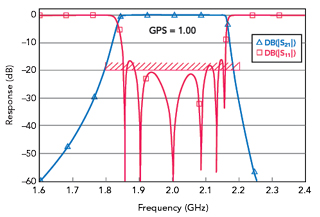
Figure 5 Simplified TEM model response with the physical GPS = 1.00 in.
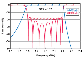
Figure 6 Simplified TEM model response with GPS’ = 1.20 in. and the modified tap position.
MICROSTRIP INTERDIGITAL AND COMBLINE FILTERS
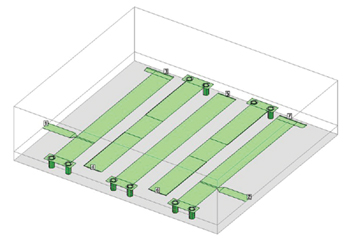
Figure 7 Alumina microstrip interdigital filter with N = 5.11
Modeling microstrip passive components has always been a challenge. The microstrip interdigital filter11 has been a very popular topology in integrated microwave assemblies due to its very compact layout. The active area of an N = 5 tapped interdigital filter in thin-film ceramic is roughly λ/4 wide and λ/4 long (see Figure 7). This is in contrast to the popular edge-coupled topology that can be several wavelengths long.
There are manufacturing issues with the microstrip interdigital filter, however, that can be quite frustrating. The laser drilled vias, often used for grounding, have a finite XY location tolerance in the substrate. The alignment of the metal pattern to the vias also has a finite tolerance. If we consider the resulting electrical length of each resonator, these tolerances can cause every other resonator to be either too long or too short. The resulting passband is then seriously mistuned.
After fighting these issues for many years, we finally seriously considered the microstrip combline. A key development was the understanding that because microstrip is quasi-TEM and we have some inductive loading at the base of the resonators and some capacitive loading at the resonator open ends, we can build useful combline filters without adding discrete loading capacitors and grounding vias at the open ends. This is a significant simplification for manufacturing.