
This article describes how trends in the aerospace and defense (A&D) industry drive power amplifier (PA) design and how device models can accurately predict the performance of GaN PAs to keep pace with increasing demands. These models are consistently verified and validated through stringent practices as RF device process technology evolves.
GaN-based power transistors have been rapidly adopted in an array of commercial, industrial and military applications for their superior performance in PAs. These devices can reduce solution size with increased power density at comparable or even lower system costs than traditional solutions. GaN solid-state PAs have been replacing other technologies such as traveling wave tubes, GaAs MMICs and laterally-diffused metal-oxide semiconductor (LDMOS) transistors in military radar applications with their ability to provide higher peak powers with wider pulse widths and broader bandwidths. This trend is seen across a multitude of applications, from satcom systems to active electronically scanned array (AESA) radars and electronic warfare systems. To fully exploit the intrinsically beneficial characteristics of these devices, RF/microwave design engineers rely heavily on their respective nonlinear models.
TRENDS IN A&D
In military radar systems, AESA phased array antennas are rapidly replacing traditional mechanically steered arrays (MSAs) and passive electronically scanned arrays (PESAs) in air traffic control, marine radar, weather radar and missile seekers. Older MSA radar systems typically use aperture antennas that sit on a gimbal to manually pivot and point the radiated beam in a desired direction for maximum transmission/reception. These systems, however, incur substantial maintenance costs due to moving parts and rotating joints that require frequent repair.
PESAs are electronically “steered” by adjusting the beam of many radiating elements, using passive attenuators and phase shifters, all of which are connected to a single transmit or receive path. A high power pulse from a central transmitter is routed through a single path and emitted from the antenna array and is then rapidly switched to a single receive path to amplify echoes from the desired target.
Unlike MSAs and PESAs, AESAs enable graceful degradation due to a diversity of transmit/receive paths, making them less susceptible to catastrophic common-mode failures. Like PESAs, AESAs are composed of multiple radiating antenna elements, enabling electronic beam steering by controlling the phase and amplitude of each element; however, each element in an AESA is an active transmit/receive T/R module with a PA for transmit and a low noise amplifier for receive. This system design not only customizes the strength and radiation pattern of the beam (e.g., sharper beam with a narrow beamwidth) but can also simultaneously search, detect and track multiple objects from different directions and at different heights.
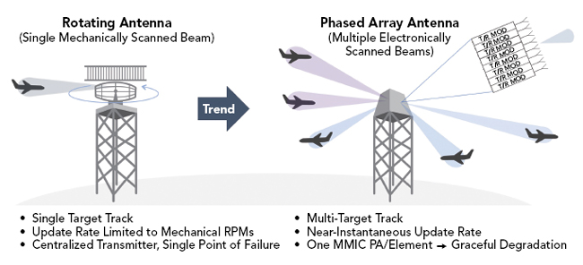
Figure 1 MSAs with rotating antennas and single beams are being replaced with multi-beam AESAs.
AESAs rely on strict amplitude and phase consistency due to the complex beamforming techniques employed, often using FPGAs for memory, processing and control. Efficiency and linearity are typically dictated by the type of modulation used in the signal to be amplified. These techniques enable real-time, simultaneous multi-object search, tracking, acquisition, identification, guidance and control with a near-instantaneous update rate (see Figure 1). This requires highly linear amplifiers with excellent amplitude and phase consistency.
These systems also have an inherent resistance to jamming, where improved beam shaping control enables considerable sidelobe suppression and a wide operating bandwidth allows the radar to hop along a wider range of frequencies. The wide bandwidth also enables a higher range resolution, a capability of increasing importance to distinguish between two or more targets on the same bearing.
Evolving A&D Market Trends on PA Design
Demonstrations of the intrinsic merits of AESAs over MSAs and PESAs in military radar are plentiful. The evolving requirements of advanced AESA radar systems, however, put strains on both the transmit and receive chains. Wide bandwidths enable high range resolution and wide pulse widths enable the radar to capture more information; GaN HEMTs and MMIC solutions have been adopted by the military over the past decade in L-, S-, C-, X-, Ku- and Ka-Band radar to achieve wider bandwidths and more power.
The design of ultra-broadband PAs often uses multiple transistors in a multi-octave PA design. This involves complex design considerations around realizing a proper matching network, as the optimum impedance varies with frequency. The impedance selected in each octave is critical for maintaining high gain and PAE. MMIC solutions typically involve the use of on-chip passive components that increase the chip area.
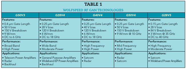
GaN on SiC technologies provide several intrinsic benefits, including high breakdown voltages (> 200 V), high saturated electron velocity, high power density (up to 9 W/mm), good thermal conductivity, low parasitic capacitances, a low turn-on resistance (RDS(on)) and thus higher power and bandwidth. Wolfspeed has developed several GaN on SiC process technologies to exploit these benefits and improve A&D system performance in areas such as phased array radars (see Table 1).
GaN on SiC offers an optimum balance of power density, cutoff frequency, maximum oscillation frequency and noise figure, allowing for smaller die sizes and simpler input/output matching networks. The typical multi-transistor, multi-octave design for GaAs and Si-LDMOS solutions can now be replaced with a single GaN solution. The simplified matching network allows higher PAEs, which, in turn, reduces electrical power consumption, PA size and cost.
Device Efficiency and Linearity
There are A&D applications such as satellite communications (satcom) that require the use of modulated signals (BSK/QPSK/OQPSK). These systems demand very linear PAs that often operate in the class (ABCF) or back-off class (ABCF) modes. GaN on SiC devices can be combined with sophisticated circuit architectures to achieve the necessary efficiency and linearity. These design methods include Doherty, envelope tracking and outphasing coupled with digital predistortion. To reduce a system’s size and resource consumption, the efficiency of the amplifier must be optimized while maintaining all other desired performance objectives. This is a challenge when having to back off an amplifier from saturation by several dB. These technical needs are ubiquitous across the frequency spectrum.
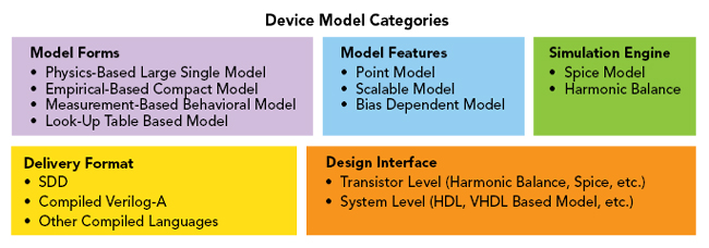
Figure 2 Device models vary in form, features, simulation engines, delivery formats and design interfaces.
DEVICE MODELS
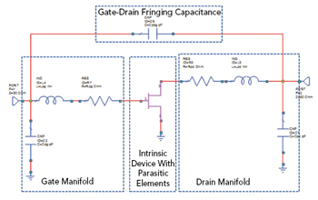
Figure 3 Wolfspeed’s empirically-based model.
The design of high frequency, high efficiency amplifiers relies heavily on the nonlinear device model used in the foundry’s process design kit (PDK). It is critical that the simulated results of the design closely match the measured results well into mmWave frequencies to effectively optimize device performance, minimize design cycles and increase device reliability.
Optimizing GaN HEMT performance with a good nonlinear device PA design and optimization requires accurate and complete simulation tools, including sophisticated models of power device behavior. This is especially true to take advantage of the high efficiency, high gain and relatively straightforward matching methods associated with GaN HEMTs.
There are several factors that contribute to what might be considered a “good” nonlinear device model for the purposes of MMIC design, including:
- Fast simulation with no major convergence issues
- Accuracy over a wide variety of sizes, geometries and bias conditions
- The ability for designers to exploit the device potential by extrapolating beyond the regions of characterization with good accuracy
- A straightforward implementation that supports various simulation platforms
- The ability to be extracted with a finite amount of data
- Simple enough for regular updates with a reasonable dataset.
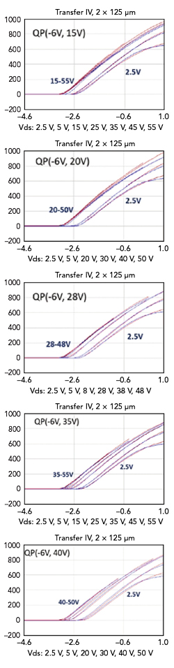
Figure 4 I-V curves showing a reduction in saturation current and a consistent shift in threshold voltage at and beyond the quiescent point.
Device models can vary in form, feature, simulation engine, delivery format and design interface (see Figure 2). With each model, there is a tradeoff between accuracy and computational speed. The physics-based model, for example, predicts device operation under various conditions (e.g., applied bias, temperature, geometries and doping levels). This can quickly become a computationally expensive process, however, with less than straightforward parameter extraction.
For this reason, a compact model is preferred, in which nonlinear ordinary differential equations are used to represent the semiconductor device behavior. Still, this is a challenge; rational approximations must be made that execute quickly with no convergence problems. It is particularly difficult to achieve convergence for devices with dynamic physical phenomena such as self-heating and trapping. Trapping occurs at a high drain voltage where electrons are injected somewhere in the GaN HEMT heterostructure, resulting in a reduction in drain current.
Empirical models simulate device behavior by using mathematically fitted equations to observed device performance characteristics (i.e., I-V, charge/capacitance). They provide a middle ground between processing time and accuracy. These models can be used universally over a variety of platforms, from higher-level analysis tools such as SPICE-based circuit simulators to more complex CAD tools.
EMPIRICAL-BASED COMPACT MODEL DESCRIPTION
Wolfspeed employs an empirical-based compact model that considers the trapping behavior of GaN devices and is accurate over several bias conditions, sizes and geometries. Models are continuously validated with evolving GaN process technologies. Because the nonlinear model is not derived from device behavior, the accuracy of the fitting procedure is key. To better represent GaN trapping behavior, the model tracks the I-V behavior of the device with different drain biases. It accurately models the optimum power/PAE load lines with drain bias changes. This is critical to provide a reliable size scaling and bias dependency. The model has two main layers, intrinsic and extrinsic (see Figure 3).
Intrinsic Layer
The intrinsic layer contains mainly nonlinear capacitances that can be implemented based in either the two-terminal capacitance form or three-terminal charge form. The three-terminal charge form is preferred, as it accounts for trans-capacitance and ensures charge continuity of the model, a necessary step to ensure the model closely matches the device’s behavior and model convergence.
The intrinsic model can be seen as virtual ports that act as voltage and current probes right at the die, while the extrinsic portion of the model includes packaging effects. The intrinsic model grants the ability to observe the voltage and current waveforms to verify the PA’s class of operation and to optimize device matching at the fundamental and harmonic frequencies.1