
While the world continues to strive for higher speed connections paired with low latency and high reliability, the energy consumption for information communications technology continues to soar. These market requirements not only position 5G for many critical applications, they also set constraints on energy efficiency and performance. 5G network performance targets impose a new set of requirements for the underlying semiconductor components, increasing the demand for highly reliable RF front-end solutions, with improved energy efficiency, larger bandwidth, higher operating frequency and smaller footprint. As the number of semiconductor devices in base station radios increases drastically, driven by the trend toward massive MIMO (mMIMO) systems, the pressure on mobile network operators to profitably deploy scarce CAPEX and OPEX resources is even more severe. Hence, limiting equipment cost and power consumption is of paramount importance for the installation and operation of an efficient 5G network.
The RF power amplifiers (PA) deployed in modern 5G radio architectures play a major role in meeting the apparently contradictory needs for ever-higher performance and lower cost. While LDMOS technology dominated the RF PAs for radio access networks in previous cellular standards, this is changing with the implementation of 5G. GaN, with superior RF characteristics and significantly lower power consumption, is a contender. There is one caveat to this storyline, however: GaN on SiC, which is predominantly being used for new 5G active antenna radios, remains one of the most expensive RF semiconductor technologies because of its non-mainstream semiconductor processing. This limits its potential for large economy of scale. GaN on Si, in contrast, combines the best of both worlds: competitive performance paired with large economies of scale, enabled by its integration into standard semiconductor process flows. In this article, we explain how advances in GaN on Si positions the technology as a very strong contender for the RF PAs in 5G radios.
5G REQUIREMENTS
The surge of digital social media, data hungry video calls and severe internet usage on mobile devices are increasing the demand for high performance 5G radio networks to provide sufficient coverage and quality of service. This trend intensified during the COVID pandemic and, consequently, operators are pushing for a sub-6 GHz 5G roll-out as an efficient way to cope with this exponentially growing data consumption. The push for higher data rates has, however, a huge impact on the global energy bill, where it is expected that information and communication technology will grow to 21 percent of global energy consumption.1
From an RF radio perspective, new 5G features translate into more challenging RF characteristics: Higher carrier frequencies to 7 GHz, instantaneous bandwidth greater than 400 MHz, higher order modulation, increased channel numbers and mMIMO antenna configuration are a few.2 Furthermore, as radios become more complex, the need to keep weight and power consumption to a minimum was never more important, with both factors demanding higher energy efficiency to save the costs of energy and cooling equipment. The RF PA stages remain mission-critical devices in 5G mMIMO radios, the last active block before air transmission, where up to 50 percent of the base station’s energy in consumed.3 Modern semiconductor technologies for RF PAs need to meet certain harsh pre-requisites to fulfill the requirements of 5G and pave the way to future generations.
In this context, GaN has established itself as the leading high-power RF PA technology for 5G mMIMO radios because of its superior RF performance. However, current implementations are cost prohibitive: GaN grown on expensive SiC wafers in III/V fabs with expensive lithography, resulting in extraordinarily high production cost compared to Si-based technologies. Initial attempts to grow GaN on Si carriers did not make it to the market because of limited performance and unfavorable cost. This is changing. In this article, we describe a new GaN on Si technology running on an eight-inch process that meets all technical requirements and offers commercially attractive economics.
RF PA TECHNOLOGIES
LDMOS — LDMOS FETs (see Figure 1) were introduced in the late 1960s to early 1970s to increase the breakdown voltage of power MOSFETs.4 The performance, ruggedness and ease-of-use of the laterally diffused structure5,6 surpassed that of Si bipolar transistors, and LDMOS became the dominant RF power technology in the 1990s.
Over the past 30 years, LDMOS has been the standard technology for the high-power transmit stages in wireless infrastructure, achieving excellent performance to 3 GHz. With the inherent cost advantage from fabricating the devices on eight-inch Si substrates and fully compatible with standard Si process lines, LDMOS has been difficult to supplant in the wireless base station market until the advent of GaN HEMTs.
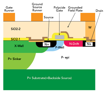
Figure 1 LDMOS device functional cross-section.
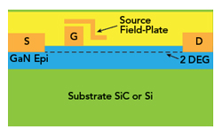
Figure 2 GaN HEMT device functional cross-section.
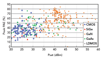
Figure 3 Psat vs. PAE vs. PA technology, measured over 2 to 6 GHz.11
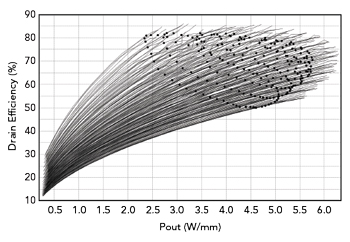
Figure 4 Load-pull drain efficiency vs. Pout for packaged 5.8 mm GaN on Si transistor.
GaN on SiC — Arising from DARPA programs of the early 2000s,7,8 which followed the successful GaAs MMIC programs of the 1970s and 1980s,9 GaN RF devices (see Figure 2) were developed to meet the demand for the higher power, wider bandwidth and higher frequency requirements of military applications, such as radar.
Compared to LDMOS, GaN has the inherent advantages of a higher critical E-field and maximum carrier density in the channel, which translates into higher power density with a higher impedance for a given output power and a lower decline in efficiency versus frequency. The attributes that make GaN attractive for military applications make GaN attractive for wireless infrastructure,10 specifically high-power density—typically 5x that of an LDMOS transistor—combined with low parasitic capacitance, which enables the device to support wider modulation bandwidths.
The market trend toward higher frequency also favors GaN transistors, which maintain higher peak efficiency as the power and frequency scale. As shown in Figure 3, GaN-based PAs are exceeding 80 percent efficiency, even above 2 GHz. These efficiency advantages are increasingly important for 5G and future communication systems.
GaN on Si — Cost has always been a major factor limiting the adoption of GaN in cost-sensitive applications like wireless infrastructure. This is especially true for applications at 2 GHz and lower frequencies where the performance gap between
LDMOS and GaN is not as significant. To address the high cost of GaN on SiC, GaN grown on Si substrates has been pursued since the early 2000s. The main challenges for performance and reliability relate to the difficulty growing high-quality GaN on Si substrates, due to lattice mismatch. A huge amount of research and development during the last 10 years, especially for power conversion applications, yielded much improved EPI quality and, subsequently, the release of many GaN on Si products, even for industrial applications.12
STATE OF GAN ON SI
Despite this progress, several challenges were overcome to demonstrate GaN on Si performance on par with GaN on SiC, as well as good reliability. Through this work, Infineon developed a GaN on Si technology for RF power that can reach its potential; after many years of development, GaN on Si is ready to become mainstream. The most important criteria determining maturity—performance, thermal resistance, reliability and cost—are discussed in the following paragraphs.
RF Performance — One of the most important performance parameters driving the replacement of LDMOS is RF efficiency. Figure 4 shows 2.7 GHz load-pull measurements of a packaged transistor with 5.8 mm gate periphery and biased at 28 V. At 3 dB compression (P3db), indicated by the circles, the peak drain efficiencies are approximately 85 percent and the peak output power density is more than 5.5 W/mm, performance on par with GaN on SiC. The contours show fairly constant efficiency from deep back-off to near saturation—making the device technology suitable for Doherty PA applications.
Thermal Resistance — One of the fundamental differences between GaN on Si and GaN on SiC is the thermal resistance, reflecting the difference in thermal conductivity of Si and SiC substrates. GaN on SiC has better thermal conductivity. However, through wafer thinning and device layout, the same junction temperature can be achieved with a GaN on Si transistor biased at 32 V as a GaN on SiC device operated at 48 V. By extension, assuming similar failure mechanisms, a GaN on Si device operating at a lower voltage will achieve the same reliability as a GaN on SiC device.
Reliability — Device failure and drift are two considerations when assessing device reliability. The mean time to failure (MTTF) is determined by the failure mechanisms, which depend on device temperature (see Figure 5). At lower temperatures, the MTTF of the GaN on Si transistor is limited by electromigration. However, electromigration is independent of the intrinsic GaN transistor, determined by the metallization and layout of the device. The MTTF due to electromigration can be extended by changing the layout. The Infineon GaN on Si device uses the same copper metallization commonly used for Si processes, which has high robustness to electromigration and achieves an MTTF of 108 hours at a temperature of 150°C.
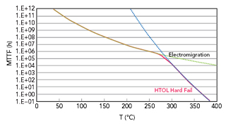
Figure 5 GaN on Si MTTF.
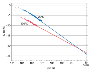
Figure 6 GaN on Si Idg drift vs. time, 25°C and 100°C.
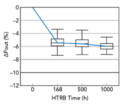
Figure 7 GaN on Si Pout drift vs. HTRB time.
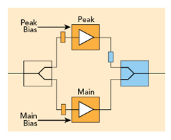
Figure 8 Single-stage Doherty PA block diagram.
Assessing the drift of the technology, Figure 6 shows the Idq drift at 25°C and 100°C with the device biased at 10 mA/mm and Vds = 28 V. Extrapolating the measurements, after 10 years the Idq drift will be less than 25 percent. Figure 7 shows the degradation in output power versus time of a 20 mm packaged transistor undergoing a high temperature reverse bias (HTRB) stress test. The device is biased at Vgs = -15 V, Vds = 100 V and the temperature is 150°C. The output power degrades less than 8 percent through 1000 hours of HTRB stress.
Cost — The cost per area of a GaN on SiC device is driven by the SiC substrate and the cost of processing typically small wafers in a III/V fab. By comparison, the Infineon GaN on Si technology runs on eight-inch wafers in a standard Si fab, since it is compatible with other silicon wafer production. The GaN on Si wafer production runs on modern, eight-inch Si production equipment, taking advantage of Si’s inherent integration, performance, yield and supply chain infrastructure. RF integration leading to more complex MMICs is a longstanding trend, so the cost per area of a volume Si fab remains an important differentiator.
GaN on Si PA MODULES
The key performance parameters for a wireless infrastructure PA module (PAM) comprise the power-added efficiency (PAE) at the nominal RF output power, the dynamic peak output power and the ability to linearize the PA in both frequency-division duplex (FDD) and time-division duplex (TDD) modes.
A trend for the RF power per antenna element in active antenna systems (AAS) is increasing the nominal linear output power of the PAM from 3 to 8 W, possibly to 12 W and higher. The frequency and antenna array scaling impose a size restriction on the PAM so it fits within the element spacing on the RF printed circuit board (PCB) to minimize the system cost. Power GaN technology supports this compact form factor because it can withstand higher junction temperatures.
To assess the capabilities of Infineon’s GaN on Si technology, a single-stage Doherty amplifier PAM on a multi-layer organic laminate substrate was designed to have an average modulated linear power of 39 dBm in the 3.4 to 3.6 GHz band (see Figure 8). In a Doherty design, the input signal is split between “main” and “peaking” amplifiers, and the amplifier outputs are recombined with a 90-degree phase shift in one path. Biased at 28 V and with a single-tone input signal, the gain and drain efficiency (DE) of the PAM versus output power were measured at room temperature (see Figure 9). At 39 dBm output, 10.5 dB power gain was achieved, including the 3 dB splitter, combiner and other passive losses. A maximum output power of 47.5 dBm was measured.