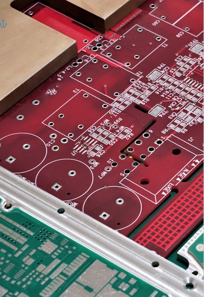
Quality Control of Post-Bonded PCBs
A post-bonded PCB is not a typical PCB, so we wanted to discuss quality control methods that we employ to ensure that the customer gets what they need.
Machining
- 100% mechanical inspection of every feature (utilizing visual and contact inspection techniques)
- Visual inspections derived from CAD data (directly from .iges and .stp files, while inspection from .dxf and .dwg files is possible with interpretation)
Sweat Solder
- X-ray inspection of the solder joint (standard): Each part is inspected for proper reflow and wetting, and void volume is evaluated, not quantified
- Visual inspection (standard): No excess solder
- Peel testing (non-standard): Empirical testing of adhesion on production parts
- Convection reflow (non-standard): Simulation of subsequent convection reflow soldering cycle and validation of product robustness
- Sonoscan (non-standard): Non-destructive test, but we currently outsource. This is a technique that can be used to get an image of the entire part and look at the void volume
Sheet Film Adhesive
- Resistance measurements
- Visual inspection that ensures no excess flow of adhesive material
Embedded Copper Coins

Coin technology is quickly becoming a preferred alternative to internal heat sinks to draw heat directly down and away from the heat-generating device to the backside of the PCB. The phrase “press fit coin” gets used quite often when discussing various embedded coin applications. The fact is that most practical applications where coins are employed use a coin that is bonded into the structure during the multilayer lamination process. In this case, the coin is bonded into place and sealed by the flow of the prepreg resin, which is adjacent to the coin at the time of lamination. The result is a securely mounted but electrically isolated coin. Either ground via structures are added through a flange in the coin, or the cap plating on the top and bottom of the coin provides the grounding connection.
We have utilized a few different kinds of coins: a center-flanged coin, a bottom-inserted coin (or a T-coin), a coin that does not go through all the layers, a U-coin, and a serrated coin. It is important to understand that every embedded coin part number tends to be a unique engineering project for a PCB board fabricator. Figure 4-9 displays a micro-section of an ASC PCB with a flange coin.
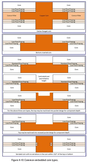
Figure 4-10 shows different types of coins. When designing, it is always preferred that the top and bottom of the coin be in a positive or near- neutral position relative to the top and bottom of the PCB. On the bottom, this ensures that intimate contact can be made with any external heat sinking. Being on the top ensures that the device typically mounted on top of the coin can be adequately solder paste printed and soldered properly to the electrically and thermally conductive structure. When you consider both aspects, it is self-explanatory that a negative condition, one with either the top or bottom of the coin recessed within the circuit board, is less than ideal. Tolerances need to be made to allow for reasonable manufacturing yields. In these cases, a preferred tolerance would be ranging from a slight negative condition of -0.0005” or -0.5 mil to a positive condition approaching +0.002” or +2 mils.
Early engagement and ongoing communication with your fabricator are essential to settle on a specific mass of coin required for the thermal dissipation necessary for device operation within the design temperature requirements. The fabricator will need to adjust the actual coin size slightly to ensure proper fitment and clearance within the pocket in the multilayer. This will also ensure proper prepreg resin fill around the coin as well as ensure that the surface flow of resin is minimized.
Reducing resin flow onto the top surface is important when using thinner copper foils on the top and bottom layers since planarization (sanding or disk grinding) is the most common method for removing excess resin flow. When fine lines and spaces are employed, there is always a tendency to use thinner copper to ease manufacturing. Half-ounce copper will, of course, be more susceptible to damage during planarization than one-ounce copper foil. One-quarter ounce copper foil will be virtually impossible to clean mechanically, so chemical or plasma methods will need to be used—both of which are capable of removing only very slight amounts of resin from the surface.