
A broadband bandpass filter design is implemented with three different topologies comparing waveguide and substrate integrated waveguide (SIW) structures. A novel SIW structure using metamaterial resonators offers the best compromise of size and performance.
Filters are necessary in telecommunications systems for separating useful signals from parasitic signals and noise.1 Due to its low loss and high power handling capability in high frequency applications such as radar and satellite communications, air filled waveguide is a popular medium.2 Because of the physical constraints and relatively high cost of traditional waveguide, however, planar technology is often preferred.
SIW offers a compromise that increases the density of integration while lowering production costs. Doucha and Abri3 demonstrated that two rows of vias between metal plates can confine an electromagnetic field as well as a waveguide. The addition of symmetric inductive irises or metamaterial4 perturbs the field in this structure and introduces a filter function to its response.
WAVEGUIDE AND SIW
Ordinary metal waveguide is a transmission line often used in the microwave domain. It is a hollow tube with generally a rectangular or circular cross section. Its main advantage over wire transmission lines is that loss is minimized. On the metal surfaces of its inner walls, the magnetic (H) and electric (E) fields are equal to zero. The fields are thus confined within a low loss air space as they propagate down the guide.5
The use of ordinary waveguide is limited by its relatively large size and cost.6 For rectangular waveguide, for example, the width (cross section) for single mode transmission is approximately half the wavelength of the transported wave (see Figure 1a):7
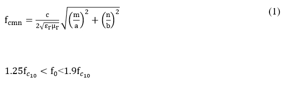
Where fcmn is the cutoff frequency for the order (m, n). The inner metal surface of the guide is often plated with silver or gold to reduce losses due to the skin effect, which increases cost.
SIW provides a solution by filling the guide with a substrate of permittivity εr and replacing the side walls with metallic vias (see Figure 1b):
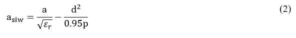
Equation (2) shows that as permittivity increases the size of the structure decreases,7 while the ability to use large scale photolithographic techniques in manufacturing reduces cost.
In microwave transmission/reception systems where the signal at the antenna must pass through a SIW structure, an intermediate transition is generally required to match modes and impedances (see Figure 1c). To add a filter function to the SIW structure, an internal discontinuity, such as a symmetric inductive iris or metamaterial, is introduced.8
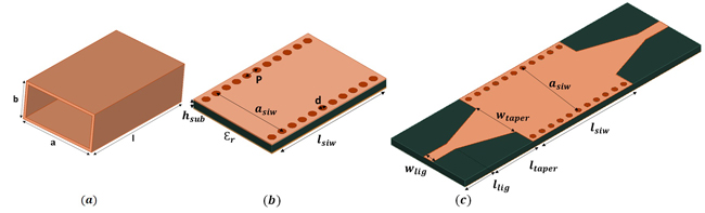
Figure 1 Rectangular waveguide (a), SIW (b), SIW transition to microstrip (c).
SYMMETRIC INDUCTIVE IRIS
A symmetric inductive iris comprises two metal plates inserted face to face inside a waveguide. It is inductive because the plates are perpendicular to the magnetic H plane and this exhibits an inductive susceptance. The inductive iris and its equivalent circuit are illustrated in the Figure 2. The following equations are used to calculate the dimensions of an n-section waveguide filter with a symmetrical inductive iris:

To design a filter for a SIW structure, it suffices to apply Equation 2 to all the dimensions and replace the guide irises with metal vias.9-10
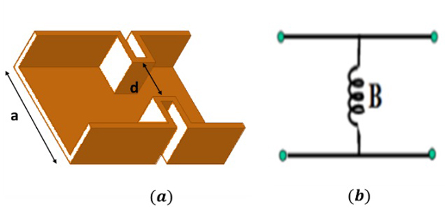
Figure 2 Inductive iris (a) and its circuit representation (b).
METAMATERIAL
The term “metamaterial” refers to an artificial composite that has electromagnetic properties not found in nature. It may also be referred to as left hand or negative refractive index material.4 The origin of these terms is due to the propagation of a plane wave through metamaterial. The trihedron formed by the vectors (k, E, H) is inverted and since permittivity and permeability are negative, the refractive index is negative as well.

Metamaterial is generally realized as a substrate plated on the bottom with another on the top etched with different geometries. It is inexpensive because it employs circuit board manufacturing techniques.11 In this article, the upper metal layer consists of four half-rings (see Figure 3). The equivalent circuit model considers each half ring as a parallel inductance, so four parallel inductors are included in the model. In addition, parallel capacitance due to the rings is also included as well as a series impedance to account for losses and power dissipation.12-13
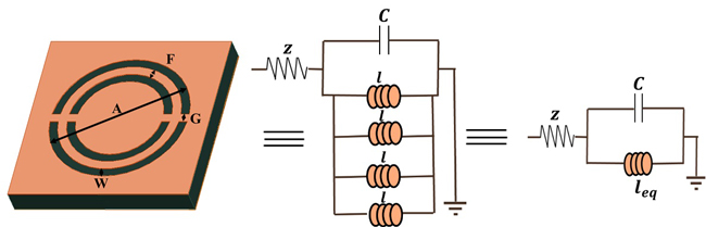
Figure 3 Metamaterial cell and its equivalent circuit.