
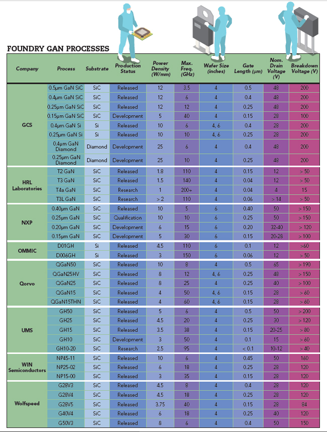
Featured in this month’s Microwave Journal, a survey of the major RF GaN fabs around the globe. The eight companies responding to our request for information offer an astounding 36 process variants (see the table at the end of this article), fabricating devices with 0.5 µm to 40 nm gate lengths on GaN on SiC, GaN on Si and GaN on diamond substrates. The process count does not include proprietary recipes the foundries maintain for their customers.
Since RF GaN became a topic at industry conferences in the mid-1990s,1 GaN has been commercialized, adopted primarily for military radar, electronic warfare and cellular base stations. One indication of the technology’s success: GaN revenue reached $1 billion in 2020, according to Strategy Analytics. Read more about the market development for GaN in the accompanying article by Eric Higham of Strategy Analytics (view here).
Eight GaN fabs responded to our survey:
- GCS
- HRL Laboratories
- NXP
- OMMIC
- Qorvo
- UMS
- WIN Semiconductors
- Wolfspeed.
Five of the eight are based in the U.S., two are in Europe and WIN Semiconductors is in Taiwan. All except for NXP are “open foundries,” willing to engage with any customer—subject to export controls for the U.S. foundries.
Most GaN on SiC processes run on 100 mm wafers, although three of Qorvo’s five processes and all NXP’s are on 150 mm GaN on SiC wafers. Wolfspeed plans to migrate to 150 mm during the “next couple of years” as volumes increase. Although wafer diameter is often used as a marketing promotion, a loaded 100 mm fab is more cost efficient than a lightly loaded 150 mm fab. Interestingly, GCS’ and OMMIC’s GaN on Si processes use 150 mm wafers, which likely reflects the maturity and availability of silicon substrates.
While volume applications for RF GaN are below 20 GHz (e.g., phased array radar and sub-6 GHz base station power amplifiers), all the fabs surveyed have or are developing shorter gate length processes to extend device performance well into the mmWave frequencies, anticipating the capability of GaN to compete with GaAs and silicon for commercial and military applications at these higher frequencies.
In addition to offering competitive device performance, open foundries must support designers and their programs with design tools and test and packaging services. Alternatively, it could be test and packaging services and design tools. The survey identified the following capabilities:
In addition to dedicated wafer fabrication, HRL Laboratories offers multi-project wafers for its mmWave T3 process, enabling prototype runs at reduced cost. HRL is a U.S. Department of Defense (DoD) Trusted Foundry and provides designers with process design kits (PDKs) for Microwave Office and ADS.
GCS provides nonlinear device modeling and RF characterization, Silvaco device simulation, thermal analysis, failure analysis, 100 percent on-wafer DC test and die inking.
OMMIC offers DC and RF on-wafer screening to deliver known-good die; visual inspection, including space grade for flight; reliability testing, including wafer and lot acceptance tests; environmental testing; and MMIC packaging.
Qorvo provides advanced packaging design, assembly and test for DoD programs, defense primes and commercial companies and meets the DoD’s Trusted Cat 1A facility requirements.
UMS offers online design rule checking, RF on-wafer testing into mmWave frequencies (e.g., S-parameters, noise, power) and packaging options.
WIN Semiconductors can accommodate custom models, testing and offers various assembly interfaces.
Wolfspeed supports ADS and Microwave Office PDKs and provides DC and RF on-wafer probing.
All the fabs maintain reliability assurance programs to qualify new processes and monitor released processes for unexpected changes that could impair the reliability of devices fabricated on their lines.
Qorvo’s GaN HEMT reliability qualification includes multi-temperature DC accelerated life testing (DCALT) and RF operational life testing, with reliability lifetime projections based on a failure criteria of less than a 10 percent change in Imax and using the 90 percent confidence lower bound for determining activation energy. Ongoing process monitoring consists of continuous DCALT monitoring using reliability test FETs on every wafer.
NXP’s reliability qualification requirements include extended testing to 3x the expected lifetimes. Although most of NXP’s GaN products are supplied to cellular base stations, the company’s manufacturing operations are certified to the stringent automotive IATF16949 quality system standard.
For OMMIC, the final step in qualifying its GaN on Si processes is a space evaluation in collaboration with the European Space Agency.
Similarly, UMS’ GaN processes are internally qualified to a minimum target of 20 years at 200°C, followed by space-level evaluation with outside space agencies.
WIN’s GaN qualification follows industry test methods, with the results documented in qualification reports, available for review by customers.
The responses to Microwave Journal’s survey reflect a strong global supply chain. These eight fabs are not the only suppliers of RF GaN devices: several “captive” fabs within defense primes serve their own programs, and compound semiconductor fabs are emerging in China (not included in this survey). RF GaN is clearly a strategic semiconductor technology.
Reference
- R. J. Trew, M. W. Shin and V. Gatto, “Wide Bandgap Semiconductor Electronic Devices for High Frequency Applications,” GaAs IC Symposium IEEE Gallium Arsenide Integrated Circuit Symposium, 18th Annual Technical Digest, 1996, pp. 6-9, doi: 10.1109/GAAS.1996.567625.