
The energy efficiency of an RF front-end (RFFE) is a vital characteristic, whether a radio is battery or mains powered. For battery powered, reducing the maximum current drawn from the battery increases the time between charges. For mains powered, important properties such as size, weight and power are dictated by the RFFE efficiency. Consequently, many amplifier architectures and inventions have been developed to minimize wasted energy in the transmitter. Although improving efficiency, some of these rely on theoretically impossible modes of operation, and some fail to fully use the device’s capabilities.
This article provides some analysis of and insight into amplifier efficiency. First, the tuned amplifier concept and efficiency enhancing mechanisms are explained. Then, the effects of each mechanism on amplifier efficiency are illustrated, revealing some surprises. The better known methods for improving amplifier efficiency are classified by their mechanisms - also noting the mechanisms not used - and identifying areas for improvement. Finally, the article shows that harmonic load-pull measurements on a device highlight its potential; using such measurement data with a look-up table, for example, amplifier performance in a variety of schemes can be predicted.
THE TUNED AMPLIFIER
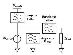
Figure 1 Simplified schematic of a tuned amplifier, class A to C.
A tuned amplifier circuit can be used to describe the continuum of amplifier class characteristics from A to C, via AB and B, based on sinusoidal voltage waveforms and quasi-linear operation. A more detailed explanation is provided in Chapter 3 of Cripps’ book.1 A simplified model of the power amplifier built around a controlled current source is shown in Figure 1. The model can be simplified into three frequency domains:
- DC current flows through the lowpass filter and the controlled current source (i.e., the device). Its progress elsewhere in the circuit is blocked by the bandpass and highpass filters.
- At the fundamental frequency, the signal current through the device passes solely to the intended load impedance (Zload), creating a voltage across the device and load.
- Harmonic currents flowing through the device are short circuited through the highpass filter, as any harmonic currents flowing in the device “see” zero impedance and do not create any voltage.
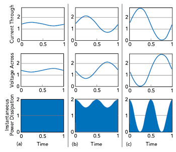
Figure 2 Class A amplifier waveforms at low (a), medium (b) and high (c) output power.
The voltage across the device comprises only DC and fundamental components and is sinusoidal. Power is dissipated by the device when a current (id) flows through it with a voltage (vd) across it and where the current and voltage overlap during the waveform cycle. For a class A amplifier, the simplest case, Figure 2 shows the power dissipation versus time at three power levels. As the output power reduces, the power dissipated waveform tends to a constant value. At higher output power, the dissipated power reduces. The power consumption is constant in all cases, and the power dissipated is the total area under the power dissipation curve. In the case of this class A amplifier, the amount of power dissipated (wasted) decreases as output power level increases, from (a) to (c).
EFFICIENCY ENHANCEMENT
How will efficiency enhancement mechanisms improve the energy efficiency? Consider classifying the mechanisms for reducing the wasted power in a tuned amplifier. These mechanisms relate only to the device itself, not to external modulating circuitry such as harmonic terminations or modulators. Three base mechanisms can enhance the efficiency of a single-ended amplifier: waveform engineering, supply modulation and load modulation.
Waveform Engineering - The shape of the voltage and/or current waveform is modified, which is what happens when passing through the class A to C continuum. Harmonic content is introduced into the current, modifying its waveform, in a predictable but restricted way.1 Alternatively, the ratio of the current’s harmonic content may be modified by injecting harmonics from either the input side or output side. For the current’s harmonic content to affect the voltage waveform, a non-zero impedance must be present at that harmonic frequency. In the limiting case, both current and voltage waveforms are square waves and antiphase. As one of them is zero at any instant in time, the power dissipation is zero. This zero dissipation applies at least to the device, but it could just be shifted elsewhere in the system.
Supply Modulation - The average or envelope supply voltage across the device, Vsupply, is modified. With a perfect device, Vsupply is the root-mean-square value of the voltage waveform, set so the minimum value of vd reaches zero.
Load Modulation - The Zload presented to the device at the fundamental frequency is modified, ideally so the voltage (vd) swings from 0 to 2 times the supply.
Figure 3 illustrates these mechanisms using a class B waveform as the reference. The class B current waveform is half sinusoidal, compared to fully sinusoidal for class A operation. The fundamental current is equal in both classes A and B when the peak-to-peak current variation is equal. The reason for using a class B waveform as the baseline is because the efficiency can be enhanced by all three methods. Class A, on the other hand, cannot be improved with load modulation alone: class A power consumption remains constant regardless of the load impedance.
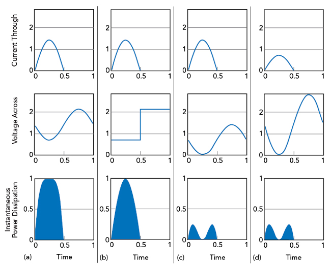
Figure 3 Efficiency enhancement mechanisms compared to a class B waveform at 6 dB back-off (a), waveform engineering (b), supply modulation (c) and load modulation (d).
Class A Case Study
One of the goals of this article is to illustrate efficiency enhancement mechanisms so they can be used optimally. The class A case is not a lost cause. Figure 4 shows the voltage, current and dissipation for a class A amplifier, illustrating that waveform engineering and supply modulation enhance efficiency, but load modulation does not. Waveform engineering can convert the class A sinusoidal current into the class B case of the half sinusoid in Fig. 4(b). Referring to Figure 3, class B efficiency could now be enhanced with load modulation.
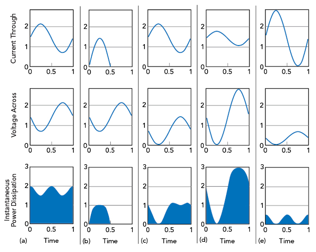
Figure 4 Class A amplifier efficiency at 6 dB back-off (a) enhanced by waveform engineering (b), supply modulation (c), load modulation (d) and an unexpected improvement using a counter-intuitive hybrid (e).
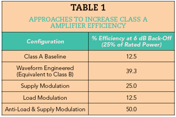
What if the device could not be waveform engineered to add the required harmonics? For example, it might be operating close to its upper frequency limit and cannot support the harmonic currents. Supply modulation in Fig. 4(c) could be used, although combining it with load modulation would be counterproductive. Load modulation increases the peak-to-peak voltage, decreasing the range where supply modulation could be deployed. Turning the problem around, if load modulation degrades the effectiveness of supply modulation, what if “unload” modulation were applied? Instead of maximizing the load impedance to maximize peak-to-peak voltage, minimize the load impedance to minimize the peak-to-peak voltage and then use supply modulation. This is the case shown in Figure 4(e), the “anti-load modulation + supply modulation” case. The peak-to-peak values of current and voltage have been completely reversed from the load modulation case, and supply modulation has been applied - achieving a quite unexpected result: the efficiency at the output power back-off of the class A amplifier has been maintained at the theoretical maximum of 50 percent.
The respective efficiencies of the five scenarios of Figure 4 are summarized in Table 1. Note that the waveforms all have the same output power.