
S-parameter data files remain the most commonly available “model” for representing passive devices in the microwave industry. Physically motivated equivalent circuit models can be set up to scale accurately with part value, substrate properties and other parameters, such as solder pad dimensions. Still, such circuit models cannot generally account for electromagnetic (EM) coupling interactions between microwave components and between components and their surrounding shielding and interconnect environment. Consequently, full-wave EM analysis has become a crucial step at RF to account for such interactions. New technology, recently available in some EM simulators, allows for encrypting geometry and material details to protect vendor manufacturing IP and enable 3D EM models to be shared with a wider design community. These advances help designers reduce design risk and re-work and improve time-to-market for today’s increasingly compact and complex product form factors.
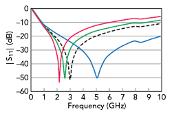
Figure 1 Simulated |S11| of an AVX 0402xU 5.6 pF capacitor mounted on three substrates vs. AVX S2P data. Blue: 10 mil Rogers 4350B substrate; Green: 30 mil Rogers 4350B; Red: 60 mil Rogers 4003C. Dashed: AVX data, measured on 20 mil Rogers 4350B.
For decades, measured S-parameter data files have been the most commonly available “model” for representing passive devices of all kinds in the microwave industry. S-parameter files, while useful, ubiquitous and very portable only represent the way a specific device behaves in the test fixture environment and the test conditions used for characterization. On the other hand, properly developed physically motivated equivalent circuit models can be set up to scale accurately with part value and substrate properties, as well as other parameters like solder pad dimensions.1 This advance is a marked improvement that is used by many designers worldwide today. However, circuit simulation is not always sufficient in terms of pre-build risk management for microwave/mmWave designs that involve compact topologies and dense circuit implementations. Accordingly, full-wave 3D EM analysis has become a crucial step to account for possible EM coupling interactions between microwave components and between components and their surrounding shielding and interconnect environment. This unexpected coupling can result in performance degradation and, in turn, lead to costly and lengthened design cycles. Assembling the necessary geometry to complete full-wave analysis that includes representations of passive elements, such as packaged and surface-mount devices as well as packages and connectors, requires close collaboration between vendors and customers of vendors and model providers. In many cases, sharing of manufacturing geometry and material details is required. New technology, recently available in some simulators like ANSYS HFSS, makes it possible to encrypt manufacturing details to better enable 3D EM models to be shared with a wider design community.2,3
S-PARAMETER FILES
S-parameter files are simply measurements of a device that are very commonly used as device “models” in high-frequency design simulations. S-parameter files are good representations of a device for simulation, provided the S-parameter measurement conditions match the design conditions. The properties of the test fixture and measurement conditions used to measure the S-parameters, such as substrate type, PCB pad dimensions and bias condition should be the same in the design to achieve the most accurate simulation. It is important to note that as frequency increases, parasitic effects become more and more significant. Thus, differences in design properties in comparison to measurement properties can lead to a less accurate simulation. Figure 1 illustrates a capacitor’s variation in S-parameter response solely due to the use of different substrates (part series, capacitance and pad dimensions are the same). While it is common for passive component suppliers to provide S-parameters for their devices, at best these represent only one possible mounting/usage scenario. In addition, measurements are typically performed in a standard coaxial-connectorized test fixture in which an air gap under the device may be present.
To evaluate different part values, pad arrangements or substrates in a design using S-parameter files as simulation models, different measurement files need to be used to represent each part value. As seen in Figure 1, the downloaded S-parameter file that represents device performance on a 20-mil substrate would less accurately predict the design response if a 10-mil substrate was used, especially for an application above 1 GHz. Another limitation to consider when using S-parameter files is that the simulation is only accurate within the measurement frequency range. Outside of the measurement frequency, an S-parameter file is generally invalid and may extrapolate to non-physical values depending on the simulator setup.
S-PARAMETER FILE-BASED MODELS
A collection of S-parameter files can be packaged together into a single “S-parameter model” for added convenience. An S-parameter model represents multiple configuration options for a device or component series. For example, it can represent multiple part values of a passive component series or simulate different bias conditions for an active device, depending on the S-parameter files included. The model includes a parameter selection menu to select the properties of the S-parameter file that should be used for the simulation, all while keeping the same model element in the schematic.
S-parameter models can also be set up to work with tuning and optimization. Two S-parameter model examples are shown in Figure 2. In Figure 2a, an S-parameter model for the Mini-Circuits EP2K+ splitter illustrates how models can be simulated on two different substrates and in Figure 2b the Gowanda C225FL conical inductor series model shows how multiple part values can be simulated without replacing the model.
Data-based or equivalent circuit models typically available often lack detailed information concerning how the measurements and/or models were developed, as well as usage information. We believe that such information is very important to designers. A model datasheet represents one way that this information can be presented. Such datasheets contain critical information concerning the model, including validation measurements along with details regarding reference planes, application/usage and more. Modelithics provides this type of detailed information for all models distributed and available for use by various circuit and system designers. The information varies based on the type of device or component represented by the datasheet; for example, different information is included in the model datasheets for the scalable equivalent circuit and 3D-geometry-based EM models discussed next.
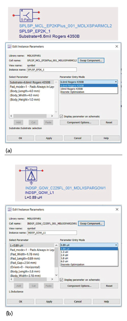
Figure 2 S-parameter models with dropdown menus to select the substrate (a) or part value (b).
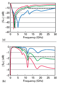
Figure 3 |S11| (a) and |S21| (b) from a scalable equivalent circuit model for an AVX 0402xU 5.6 pF capacitor on three different substrates vs. AVX S2P data. Blue: 10 mil Rogers 4350B; Green: 30 mil Rogers 4350B; Red: 60 mil Rogers 4003C; Dashed: AVX data, measured on 20 mil Rogers 4350B.
SCALABLE EQUIVALENT CIRCUIT “GLOBAL” MODELS
A scalable equivalent circuit model represents a much more efficient and powerful type of component simulation model. These models are designed and validated using S-parameter data, and oftentimes other measurements, to build a comprehensive model for a device series that scales continuously over part value ranges and other design parameters. Modelithics uses the term “Microwave Global Models™” to represent its unique approach to scalable equivalent circuit models for microwave devices. In addition to part value, these scalable global models are set up to scale with pad dimensions, substrate properties (e.g., height and dielectric constant), and if applicable, temperature, bias and other properties. The unique and advanced scaling capabilities give them numerous advantages over previously discussed file-based models.
Compared to file-based S-parameter models that represent only a set number of simulation conditions, scalable equivalent circuit models represent an extremely broad range of possibilities in terms of design properties. These models accurately simulate broadband device and parasitic behavior for many embedding configurations. In general, since the models are based on a physically meaningful equivalent circuit topology, they remain physically valid when extrapolating and interpolating parameters. That is, equivalent circuit models will exhibit physically meaningful and reasonably correct behavior even beyond the measurement frequency range. Figure 3 corresponds to Figure 1, but with the frequency sweep extended to 30 GHz. The simulated S-parameters from the scalable equivalent circuit model reveal a continuation of physical behavior on each substrate for the full frequency sweep (and beyond). The S-parameter file, which has a maximum frequency of 10 GHz, extrapolates as a straight line and is not valid above 10 GHz.
To illustrate the concept of a physically motivated equivalent circuit model, Figure 4 depicts a surface-mount inductor mounted on a microstrip substrate. Also shown is a simple equivalent circuit that can be fit to the measured S-parameters of the part up to and including the first self-resonance. Scalable Microwave Global models can be likened to multi-faceted extensions of this approach in which additional elements are added to the circuit to represent higher-frequency and higher-order-resonant behavior. Complex equation sets are incorporated to add the scalability features discussed. In addition, the resistive loss is typically fit to effective-series-resistance measurements made with separate equipment, such as an impedance analyzer or resonant line.
Compatibility with statistical analysis evaluations is another advantage associated with scalable equivalent circuit models. Component tolerance values can be set, making it possible to perform a full design yield analysis.4 If the yield is unacceptable, one can simply test different part tolerances until the most efficient and acceptable design is achieved. With suitably arranged scalable models, this design “testing” is executed quickly at the simulation stage, thereby saving time and cost incurred with extra board runs and redesigns.
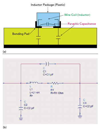
Figure 4 Surface-mount inductor parasitics (a) and first-order, physically motivated equivalent circuit model (b).
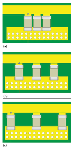
Figure 5 Three capacitors in a shunt configuration on a 50 Ω line: 10 mil spacing (a), 42 mil spacing (b) and 74 mil spacing (c) between them.