
Technical Feature
A High Efficiency, Low Cost Silicon Bipolar GSM Dual-band PA Module
T. Johansson, P. Lundin, J. Engvall and D. Uggla
Ericsson Microelectronics AB
Kista, Sweden
U. Hagström
Ericsson Microwave Systems AB
Mölndal, Sweden
As the wireless communication business continues to expand, there is great demand for reducing the cost of all parts of the systems, and to use semiconductor manufacturing processes and component techniques that can handle very high volume production during the short product cycles of many of the new devices. For a long time, the transceiver blocks in mobile phones have been designed preferably in bipolar silicon technology (RFIC), or BiCMOS if more complexity (integration level) is needed. However, for the output power amplifier (PA), III-V based semiconductor devices are still dominating, either as discrete devices, moderately integrated in MMICs, or in ceramic/PCB modules. With bipolar silicon processes offering unity gain cutoff frequencies (fT) values well over ten times the operating frequency, silicon now has the chance to compete in the PA area.
Integrated power amplifiers (IPA) fabricated in bipolar silicon or BiCMOS technologies have only recently found their way from the R&D lab to commercial applications. Excellent performance of discrete transistors has been demonstrated in both bipolar RFIC processes1 and CMOS,2 showing the potential for these technologies. For high volume GSM systems, high performance IPAs have been demonstrated using designs with on-chip transformers.3,4 However, no data on multi-band IPAs on silicon is yet available.
IPAs can generally be found in two categories of packaging: MMICs, using plastic packages (QSOP, MLP, for example) and usually with integrated heatsink/exposed ground area; or hybrid modules with matching components integrated, possibly containing several chips of different technologies. MMICs offer lower packaging costs, but require the design of a low loss matching network on the circuit board, adding passive components (increased bill-of-material) and the need for a skilled RF engineer. The hybrid modules are larger than the corresponding packaged MMIC (for example, a 9.1 x 11.6 mm footprint compared to a 5 x 5 mm footprint for an MLP package), but provide higher yield and lower total system costs by offering ready matched (to 50 W) input and output, and part of the other necessary components integrated into the modules. PA modules have, therefore, gained in popularity for inclusion in radio designs, as the handheld devices are getting smaller, the design cycles shorter and the increase use of subcontractors, with fewer available designers skilled in the art of RF-PCB design.
The commercially available state-of-the-art modules for GSM dual-/ triple-band are fabricated using GaAs HBTs. Typically, 55 percent power-added efficiency (PAE) for GSM900, 50 percent for GSM1800 and 45 percent for PCS1900 are obtained, while meeting their other specifications.
However, the GaAs-based HBT modules may have problems meeting very high volume requirements and future price reductions. Feasibility studies of similar modules based on silicon technology are therefore needed.
An integrated bipolar silicon-based dual-band PA PCB module was presented in 1998.5 Using discrete transistors fabricated in an RFIC process, PAEs of 46 percent at 900 MHz and 38.6 percent at 1750 MHz were obtained.
To the best knowledge of the authors, the data in this article is the first one presented for a dual-band module based on silicon technology that can match the performance of commercially available GaAs HBT-based modules.
Active Device Technology
|
|
|
Fig. 1 The 1.4 x 2.5 mm silicon PA chip. |

As opposed to the modules available in the market today, where several III-V technology HBT amplifier chips are mounted together, possibly with a silicon (CMOS or bipolar) control chip, the heart of the module presented in this article consists of a single silicon bipolar RFIC. This gives an advantage for further downsizing the module's geometrical dimensions. The semiconductor process used for the silicon PA chip is a 0.5 mm, 25 GHz fT , double-poly silicon bipolar process with additional features for improved wireless performance (Wireless-Trench™).6 It allows operation up to 5 V, and includes NPN and PNP transistors for analog and digital designs. Integrated capacitors and inductors are used for on-chip integrated internal matching networks. Four layers of metallization with a thick top layer for improved performance of the passives are used. Advanced deep trench isolation is used to obtain small-size, low parasitic devices in high performance processes. Special front-side metallized substrate contacts provide excellent ground paths from active devices to the highly doped semiconductor substrate and package ground.
A dual-/triple-band (GSM900, GSM1800 and PCS1900) chip was designed and fabricated in this technology. Dual two-stage power amplifiers, one for the low band and one for the high bands, are integrated on the chip together with input and interstage matching. Output matching is done off-chip. The chip also includes circuitry for analog power control, band-select (GSM900 or GSM1800/PCS1900 active) and a digital control signal for power down mode. The area of the chip is 3.45 mm2 . It can be used in an IC-package with external output matching on a circuit board, or in a module as described in this article, where output matching and some of the passive devices of the supply network are included. A photo of the chip is shown in Figure 1 .
Matching Network Design
Since the silicon PA chip had been designed with Cadence Analog Artist, and Agilent ADS was going to be used for the matching network and module designs, the circuit data and SPICE model information were transferred to the ADS environment. The power control circuitry was replaced by simple voltage sources. From these inputs, a set of small-signal S-parameters for the amplifiers were obtained from ADS, and used to estimate the elements of the output matching networks. Calculations, using the S-parameters and Smith charts, showed that a one-section matching LC network was easy to realize, but as the transformation ratio in the network was larger than ten, it could cause a narrow bandwidth. However, a two-section network gave component values that were considered difficult to realize, so a one-section LC-type network was decided upon for the output matching.

Fig. 2 Optimized values of the matching elements; (a) GSM900 amplifier module and (b) GSM1800 amplifier module.
Using ADS, the stability of the amplifiers was checked and they were found to be unconditionally stable. The optimization function in ADS was then used with starting values for L and C obtained from the previous LC network calculations to obtain matching parameters for the equivalent circuits shown in Figure 2 . The supply voltage was set at 3.4 V, and the input inductance L5 and power supply connection L6 were estimated to be 1.5 nH (one bondwire, 1.5 mm length). The output matching values obtained were 1.89 nH and 16.7 pF for the GSM900 amplifier, and 0.94 nH and 7.44 pF for the GSM1800 amplifier.
Using these parameters, the expected PAE and output power were calculated. Since the harmonics (nf0) may contain considerable power, the calculations were done for harmonics up to 4f0. The peak PAEs were estimated to be 56.4 percent for GSM900 and 46.2 percent for GSM1800, while the saturated output powers were estimated to be 34.2 and 33.3 dBm for GSM900 and GSM1800, respectively.
Module Design
The module design was focused on the output matching networks, RF chokes to the supply voltage, and access for the analog and digital control signals, since the silicon PA chip already contained the input and interstage matching networks. The design goal was to obtain maximum PAE, without sacrificing other important parameters such as output power and gain.
Substrate Material
For this experimental design, a double-layer ceramic substrate was chosen with a thickness of 15 mil. Although PCB or thicker (25 mil) ceramic is somewhat less expensive, the design goal for this study was size, and the thin ceramic leads to smaller layouts. Only one conductor layer (25 mm thick) was needed for the matching networks and connections. The silicon PA chip was mounted on the substrate using conductive glue, and wire-bonding was used for the connections. The design rules for the conductive patterns on the ceramic substrate did not pose any special limitations on the layout. For this demonstrator module, no considerations about how to protect or encapsulate it (plastic overcoating or lid) were made.
RF Chokes
|
|
|
Fig. 3 Module pattern layout; (a) integrated RF chokes and (b) discrete RF chokes. |

Two different approaches for the RF chokes to Vcc (L3) were tested. In the first layout, the chokes (inductors) were integrated on the substrate using microstrip lines, while in the second layout, discrete components were used. The exact inductance values for the chokes should not be critical - a typical minimum target value would be at least 2 nH for this design. The microstrip simulations were made with Momentum. The S-parameters from the Momentum simulation were then inserted in a model-based device in the schematic part of ADS, and from that model, the corresponding inductances were found. For GSM900, a final inductance value of 3.4 nH was used, and for GSM1800, 4.1 nH.
Output Matching
The simulations in the schematic part of ADS had shown the inductance needed on the output to achieve maximum PAE. However, an actual amplifier would need some degree of tuning, and the layout of the output matching networks, which consisted of an inductor on the module's substrate and a mounted DC-blocking chip capacitor, were designed so that the matching could be varied over a large range. The simulated target value for GSM900 was 1.9 nH, and an inductor with a total value of 3.2 nH would give sufficient potential for correct tuning. For GSM1800, the corresponding values were 0.95 and 1.9 nH.
Resulting Module Design
The resulting module design patterns are shown in Figure 3 , one for integrated RF chokes, and the other for discrete soldered RF chokes. In the center is the mounting area for the silicon PA chip. The RF inputs and control signals are attached from the lower side. The RF outputs and matchings are situated to the right for GSM900 and to the left for GSM1800, while the supply voltage connection is from the upper side. All connections are made from the backside of the substrate using via-holes. The area of the backside not needed for connections to the evaluation PCB card was used as ground plane.
The size of the designed module was 8.5 x 9.7 mm, which is smaller than the commercially available sizes of 9.1 x 11.6 mm. As can be observed, the layout still has potential for further size reduction.
Results
|
|
|
Fig. 4 Test PCB board for module testing. |

Test Board and Measurement Setup
To test the module, a PCB test card, shown in Figure 4 , was designed. It includes SMA-connectors for RF input and outputs, and connections for the control signals. The widths of the RF input and output lines were calculated in the same way as for the module, but with the electrical parameters (er , tand) of the PCB. The VCC input conductor width was made quite large to minimize the resistive losses. The layout of the control signal path to the module was placed according to space and width consideration of the RF signals to avoid crosstalk. The via-holes in the test card to its grounded back plane were placed almost directly under the via-holes in the module to minimize the resistive losses.
Tunings and Optimizations
Measurements were made at 900 and 1800 MHz using the setup shown in Figure 5 . In a series of experiments, the matching capacitor for the output, DC-blocking capacitors for the output, RF choke inductors (both discrete and integrated) and decoupling capacitors were varied and the characteristics of the amplifier module, with regards to PAE, output power and gain, were recorded. All optimizations were done with maximum PAE as the primary goal.
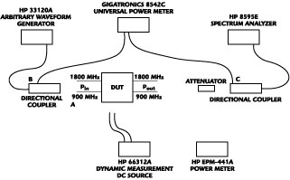
Fig. 5 RF measurements setup for module testing.
For the output matching capacitor, a value of 16 pF (obtained by paralleling two 8.2 pF capacitors) was found to give maximum PAE with enough output power (34.5 dBm) to meet the specification set for the GSM900 amplifier. Similarly for the GSM1800 amplifier, 5.6 pF was found to offer good PAE while still achieving the required output power performance. By changing the position of the capacitor along the matching choke, the performance peak was tuned to the correct frequency. Tuning results from optimization of the GSM900 amplifier are shown in Figure 6 .
|
|
|
Fig. 6 Power added efficiency for different output matching networks at 900 MHz. |

For the DC-blocking capacitors, lowest losses should be found using capacitors with a resonance frequency (obtained from the manufacturer's data sheet) matching the operating frequency because the RF signal will see the DC capacitor as purely resistive. In practice, the largest improvement of PAE between 2 and 5 percent for the different bands was obtained, using capacitors with a slightly higher resonant frequency, most likely because of the additional series inductance arising from the discontinuities of the microstrip and the via-holes. The obtained optimum values were 39 pF for GSM900 and 8.2 pF for GSM1800. To maximize the PAE, high Q components were chosen for the capacitors in the final design.
The fixed values for the designed integrated RF choke inductors, 3.3 and 4.0 nH, turned out to be too low for optimum PAE. Using the module with discrete inductors, optimum PAE for both frequencies was obtained by using 10 nH soldered chip inductors. The difference in PAE for GSM900 was around 11 percent using the best discrete inductor, while 3 percent was gained by using the best discrete inductor for GSM1800. However, optimized integrated inductors should give higher PAE because of their higher Q-values compared to discrete chip inductors.
Finally, the effect of adding decoupling capacitors at the power signal and at all external signals, compared to no decoupling capacitors, was measured. The results show that adding capacitors has little effect, most likely due to the extended internal decoupling capacitors in the PA chip. However, they may have influence on parameters such as isolation and harmonics, although this was not evaluated in this study.
Final Results
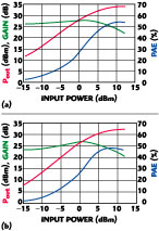
The best results were obtained with the PA module shown in Figure 7 . The PAE and output power characteristics are shown in Figure 8 . The output power reaches 34.5 dBm for the GSM900 amplifier and 32.2 dBm for the GSM1800 amplifier, while the maximum obtained PAEs are 54.4 percent (GSM900) and 48.1 percent (GSM1800). The PAE and output power figures obtained agree well with simulated values from ADS, except for the output power level for GSM1800, which is 1 dBm lower than expected. This may be because, at the higher frequency, the losses caused by the parasitic elements of the connections are larger than modeled. The maximum gains, 28.2 dB for the GSM900 amplifier and 26.6 dB for the GSM1800 amplifier, were reached at Pin ~2 dBm, and agree fairly well with the simulations.
|
|
|
|
Fig. 7 Best PA module's (a) placement of passive devices and (b) actual device. |
Fig. 8 Output characteristics for the optimized PA module for (a) GSM900 and (b) GSM1800. |

Data obtained from vendors' data sheets for commercially available modules in GaAs and GaInP HBT technology are listed in Table 1 , together with data from this work (the data are taken at slightly different supply voltages, but this should not significantly affect the listed PAE values). As can be seen from the table, the silicon module described shows competitive performance with existing GaAs technology.
|
Table 1 | ||||||
|
|
|
GSM900 |
GSM1800 | |||
|
|
VCC |
PSAT |
PAESAT |
PSAT |
PAESAT | |
|
This Work |
Dual-band Module |
3.4 |
34.5 |
54.4 |
32.2 |
48.1 |
|
Ericsson |
MMIC |
3.2 |
34.6 |
54.3 |
32.1 |
40.7 |
|
Anadigics |
triple-band module |
3.2 |
34.5 |
55.0 |
31.5 |
50.0 |
|
Anadigics |
triple-band module |
3.5 |
|
55.0 |
|
50.0 |
|
Conexant |
dual-band module |
3.2 |
35.0 |
55.0 |
32.0 |
50.0 |
|
Conexant |
triple-band module |
3.5 |
35.0 |
55.0 |
32.5 |
50.0 |
|
RFMD 3108 |
triple-band module |
3.5 |
35.0 |
55.0 |
32.0 |
50.0 |
Cost Estimates
A cost comparison with a well known, widely used GaAs PA module shows a reduction of nearly 50 percent in manufacturing cost for the technology described in this article. The substrate cost is comparable between the two technologies. The cost for passive components is decreased from $0.38 to $0.03. Only six low tolerance ceramic capacitors are needed. All inductances are integrated on the IC or on the ceramic substrate.
The main cost saving comes from the considerably lower cost of the IC. One Si chip of 3.45 mm2 in the new technology replaces two chips in today's technology (GaAs PA chip, area 3.36 mm2 , and CMOS controller chip, area 1.68 mm2 ). With an estimated cost for GaAs of $2000/100 mm wafer and Si CMOS $2000/200 mm wafer, the cost for the two chips is $1.36. With the new technology, the IC cost is lowered to $0.36.
Adding costs for mounting, molding, chip dicing, yield, test, and tape and reel packaging results in a total manufacturing cost for a module in today's technology of $2.47. The new technology as described in this article will have a manufacturing cost of $1.29, which gives it a clear cost advantage.
Conclusion
This article has reported on the design and measurement data of a PA module using silicon RFIC bipolar chip technology on a simple ceramic substrate. The data obtained show that competitive performance with the existing GaAs technology can be obtained using available silicon technology. Cost estimates also show a clear advantage in the manufacturing cost compared to today's GaAs-based modules. Cost savings have primarily been made by using silicon IC technology, and in part by integrating more functions on the ceramic substrate. Furthermore, the module also has great potential for further downsizing its dimensions, and will be able to offer a very competitive price because of its low bill-of-material. Work is now on-going to refine the prototypes into commercial products for the GSM PA module market.
References
1. F. van Rijs, H.A. Visser and P.H.C. Magnee, "Record Power-added Efficiency of Bipolar Power Transistors for Low Voltage Wireless Applications," IEDM Technical Digest , 1998, p. 957.
2. C. Fallesen and P. Asbeck, "A 1W 0.35 mm CMOS Power Amplifier for GSM1800 with 45 Percent PAE," Solid-State Circuits Conference 2001, Digest of Technical Papers , p. 158.
3. W. Simburger, H.D. Wohlmuth, P. Weger and A. Heinz, "A Monolithic Transformer-coupled 5 W Silicon Power Amplifier with 59 Percent PAE at 0.9 GHz," IEEE Journal of Solid-State Circuits , Vol. SSC-34, December 1999, p. 1881.
4. W. Simburger, A. Heinz, H.D. Wohlmuth, J. Bock, K. Aufinger and M. Rest, "A Monolithic 2.5 V, 1 W Silicon Bipolar Power Amplifier with 55 Percent PAE at 1.9 GHz," Proceedings of the IEEE International Microwave Symposium 2000 , p. 853.
5. R. Parkhurst, D. Weber, B. Jansen, W. Fang, N. Hendin, J. Kolk and M. Repeta, "Silicon Bipolar 3 V Power Amplifier for GSM900/GSM1800 Handsets," Proceedings of the BCTM 1998 , p. 117.
6. T. Johansson, "Wireless-trench Technology for Portable Wireless Applications," Ericsson Review , January 2001, p. 6.
T. Johansson is an expert on RF transistor and process design at Ericsson Microelectronics AB in Kista, Sweden. He spent several years developing high power transistors for basestation transmitters and now shares his time between advanced semiconductor process development for wireless products and development of power amplifiers in silicon for handhelds. He joined Ericsson in 1989 and holds a PhD in electronic devices from Linkšping Institute of Technology, Sweden. He has published some 35 journal and conference papers and holds 16 patents. He can be reached via e-mail at Ted.Johansson@mic.ericsson.se.
P. Lundin studied electrical engineering at University of GŠvle, Sweden. He is currently working as a test system designer for Bluetooth modules at Ericsson Microelectronics AB.
J. Engvall earned his PhD in physics from the Lund Institute of Technology, Lund, Sweden, in 1995, on studies of SiGe heterostructures. That same year he joined Ericsson. He currently holds the position of RFIC and PA design manager at the Kista RFIC Design Center of Ericsson Microelectronics AB, Kista, Sweden. He has published some 20 journal and conference papers.
D. Uggla is responsible for business development at Ericsson Microelectronics AB, Kista, Sweden. His background is in IC design engineering and he holds a MSc in physics from Linkšping Institute of Technology, Sweden.
U. Hagström studied electrical engineering at University of Gävle, Sweden. He is currently working as a radio designer at Ericsson Microwave Systems AB. His most recent project is the development of a 6 GHz WLAN system.