
A 1.5 to 2.6 GHz broadband power amplifier (PA) based on a GaN HEMT is designed to achieve high-power and efficiency. The transistor’s gate-source parasitic effect is reduced with a novel parasitic compensation circuit at the input. To achieve a broadband harmonic match and expand its bandwidth at the fundamental, radial microstrip theory is employed in a harmonic control network. The output power is between 43.4 and 45.6 dBm, and its drain efficiency is 65 to 76.9 percent from 1.5 to 2.6 GHz. Gain is above 10 dB. Second and third harmonic suppression levels are −15.6 to −26.1 and −19.4 to −40.5 dBc, respectively. The measured results are consistent with the simulation.
With the development of wireless communication technology, the need for higher data rates and correspondingly wider bandwidths is growing rapidly. At the RF transceiver, this puts a greater demand on the PA. As it consumes the most prime power, PA efficiency has a large impact on the operating budget of a communications system.
Traditional PAs, i.e., classes A, AB and B, are inefficient. To save energy and increase signal coverage, communication system PAs usually employ high efficiency and high output modes, such as classes D,1 E,2 F3-5 and inverse class F.6 They also leverage the excellent performance of third-generation semiconductor transistor technology, such as GaN HEMT.7-8
CLASS F PA ANALYSIS AND DESIGN
Since the PA operates in a large signal state, harmonics are inevitably generated, reducing output power and efficiency. Class F PAs, however, achieve good performance through harmonic control. The voltage and current waveforms at the transistor drain are shaped with a harmonic control network so the voltage waveform is a square wave, and the current waveform is a half sine wave. The waveforms of the drain voltage and current are expressed as
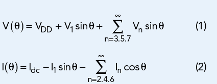
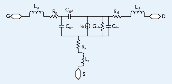
Figure 1 GaN HEMT model.
According to theory,5,9 even harmonics are matched to 0 Ω, odd harmonics to infinity and the fundamental to 50 Ω. Due to deficiencies of the class F PA in practical designs, this work describes two improvements: one, because the gate-source parasitics of the GaN HEMT transistor degrade the output power and efficiency of the PA, a gate-source parasitic compensation circuit is employed. And two, because the traditional class F PA uses a high Q output impedance matching transformer, limiting its bandwidth, this work uses low Q radial microstrip lines to control harmonics.
Gate-Source Parasitic Compensation
The GaN HEMT used in this article is an active nonlinear device, with harmonics caused by its parasitics. Gate-to-source parasitics cause the input of the transistor to deviate from a pure sinusoidal wave, reducing PA performance. The transistor model, shown in Figure 1, includes the parasitic as well as intrinsic elements. Gate-source parasitic parameters include the gate-source capacitance, Cgs, gate parasitic inductance, Lg, and parasitic resistance, Rg. Cgs is given by the expression
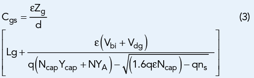
where ε is the dielectric constant of the GaN material, and d is the equivalent depletion depth. The gate parasitic inductance and parasitic resistance are found from
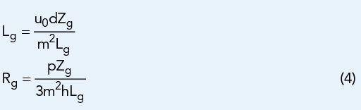
where m is the grid index, u0 is the permeability in a vacuum and ρ is the conductivity of the gate metal.
The gate-source parasitic parameters are calculated from Equations 3 and 4 and are used in the design of the input circuit (see Figure 2). Microstrip lines TL2, TL3 and TL4 compensate for the influence of Cgs at the input, where the use of stepped-impedance matching increases the bandwidth. Microstrip line TL1 offsets the effect of parasitic inductance Lg and resistance Rg. The gate-source compensation suppresses the input harmonics, which increases output power and efficiency.
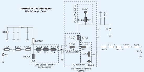
Figure 2 PA matching circuit design.