
Technical Feature
Advanced RF Technologies for the Wireless Market
Yvan Droinet
Philips Semiconductors
Caen, France
Most products in the wireless world require more and more miniaturization. This incentive leads integrated circuit designers to develop innovative architectures with higher and higher integration levels. On the one hand, there is a trend to replace more external components with their on-chip equivalents. On the other hand, however, the ultimate objective is to maximize the integration level between antenna and data output.
An important transition, from voice-oriented wireless products to data-oriented products, will occur this year. A significant number of General Packet Radio Service (GPRS) handsets will be shipped and the first applications, such as location services and credit security, will be deployed. GPRS is ready to be deployed and is a key element in bridging the gap between second generation (2G), voice-centered mobile phones and multimedia-oriented products of the third generation (3G).
|
|
|
Fig. 1 A schematic of the NZIF architecture. |

Before providing the highest bandwidth offered by 3G, a smooth evolution and a higher data rate will first be achieved with GPRS and Enhanced Data Rate for GSM Evolution (EDGE) (also called 2.5G).
The 'voice-oriented' global system for a mobile communications (GSM) handset has become a consumer product, which underlines the necessity to focus even more on a new architecture to reduce cost, size and component count. The requirement for multi-mode, multi-standard extends the GSM range in terms of service offerings. It becomes mandatory for the electronics within a handset to be designed to meet both voice and data requirements. This is a key requirement for the development of new products and increases the pressure on silicon chip vendors to provide cost-optimized, highly flexible integrated solutions, addressing the market needs of small size, feature-rich and low cost products. With the present wireless market evolution and new features such as Bluetooth, PDA and MP3, one of the keys to success is to propose a size-optimized solution able to integrate more and more electronics within the handset. Eventually, a dual-mode GSM/UMTS (Universal Mobile Telecommunication System) handset will have a form factor similar to any phone. This emphasizes the need for high performance technologies to respond to these new challenges caused by multimedia feature integration.
This article provides an overview of the different architectures available for transceiver ICs with greater emphasis on the near-zero IF (NZIF) configuration, describing different ways to interface with standard baseband devices. The second part focuses more on technology and some key design issues, linked to future product development, such as dual-mode GSM/UMTS. How to implement new functions, such as a VCO and fractional synthesizer, onto the silicon chip will be shown, providing leading edge products in terms of bill of material (BOM) and PCB size. The final section deals with the future and presents one view of how RFICs could evolve in the wireless landscape.
NZIF Architecture for 2G and 2.5G Products
|
|
|
Fig. 2 Classical dual-conversion receiver schematic. |

The NZIF architecture was introduced some time ago but very few applications have used it thus far. At the present, several devices using this architecture are in production and some of them are addressing the cellular market, such as triple-band GSM900/1800/1900 RF products, providing GPRS and EDGE (down link) capabilities.
The NZIF architecture, shown schematically in Figure 1 , differs from a classical dual-conversion receiver, shown in Figure 2 . It uses a single down-conversion receiver to a very low frequency (in RF terms), saving the space consuming and costly external surface acoustic filter (SAW) in the first IF stage.
The zero intermediate frequency (ZIF) receiver, shown in Figure 3 , also eliminates the need for an external IF SAW filter by down-converting directly the RF signal to zero frequency (DC). However, it is prone to DC errors caused by leakage of the local oscillator signal into the RF (which varies with physical handling of the phone) and by strong nearby interferers (especially amplitude modulation interferers such as TV broadcasts) that saturate the mixers.
The actual solution to cope with ZIF architecture is to significantly increase (up to 20 dB) the dynamic range required in the A/D converter to allow the DC offset to pass through and then filter it in the digital signal processor (DSP). Another solution either requires increased performance (such as IP2) in the receiver chain or the removal of the DC offset within the RF section before going to the A/D converter. Both solutions are complex, difficult to design (both from an IC and handset point of view) and not necessarily optimized in terms of an overall chipset solution.
|
|
|
Fig. 3 Schematic of a zero IF receiver. |
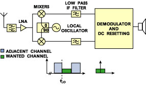
In conclusion, a GSM product using ZIF architecture must be very careful to handle the DC offset all along the receiver chain. This complexity leads to a penalty in terms of product cost (RF as well as baseband, due to the additional signal required for the DC offset) and also in terms of a key factor for success in such a dynamic industry - time-to-market.
This DC offset compensation will be even more complex to achieve in future products having higher data rates, especially with EDGE.
For the IF filter integration, the NZIF architecture makes powerful use of the polyphase technique, discriminating 'positive' or 'negative' frequencies, making this filter implementation very simple. It is now made programmable, in either GSM/GPRS or EDGE mode, by optimizing the filter characteristics in each mode.
The only point to be considered with this technique is the need for an A/D converter with twice the bandwidth (compared to a traditional double conversion or ZIF architecture). The additional signal processing capability necessary in the DSP to cope with a NZIF RF is a minor issue. All possible ways to interface with NZIF RF will be explained in the next section.
How Does the NZIF Interface to Baseband
|
|
|
Fig. 4 NZIF interface solution within the baseband. |
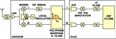
An example of the NZIF implementation shows how the signal processing is implemented within the OneC™ baseband circuit (see Figure 4 ). The analog output signal from the receive path is fed into the A/D converter, then a digital derotation is performed and low pass filtered. The main advantage from this hardware implementation is that it does not require any changes in the A/D as well as the filter characteristics, as implemented to interface with classical double conversion architecture.
Another (software) implementation is also feasible but requires modifications on the A/D and the filter bandwidth in order to cover the NZIF filter characteristics. This configuration is shown in Figure 5 . The advantage of this implementation is that an optimal reuse of a solution that is also capable of interfacing with standard architecture is made but requires the use of a complex software filter. Another optimized way, shown in Figure 6 , requires a hardware modified A/D to be converted to a true complex one with a polyphase filter integrated within the converter. This solution is fully optimized in terms of software and hardware implementation and consequently from the whole chipset and system point of view. This shows that even if 'complex' figures must be dealt with, the real hardware or software implementation is not as complex as anticipated.
|
|
|
Fig. 5 Software baseband implementation including NZIF architecture with complex signal processing only on the RF chip and DSP. |

|
|
|
Fig. 6 Hardware baseband implementation including NZIF architecture with complex signal processing down to baseband. |

New BiCMOS Technology for 3G RF ICs
|
|
|
Fig. 7 A cross section of the QuBIC4, 0.25 mm BiCMOS for 3G wireless receiver chips. |

The 3G standard will increase further the demand for RF circuit miniaturization but also for the other parts of the semiconductor circuits within the handset.
Some time ago, the market required a dual band GSM/DCS to have the same size and BOM as a single-band equivalent version. The same requirement can be expected with a dual mode GSM/W-CDMA handset, if technology evolution is considered. For this product to be consumer-oriented, the development of the new products must be started with state-of-the-art technologies to answer market needs.
As an answer to these new challenges for the IC designers and handset manufacturers, a new process has been developed to respond to their needs. The new requirements for such products are lower cost and even higher integration level, lower power or higher speed at lower current, CMOS and RF passive components for RFCMOS capability, and inclusion of SiGe as an option with minimum added masks and compatibility with a 0.25 mm standard CMOS process.
A new 0.25 mm BiCMOS process, QuBiC4, was developed with the following features:
- Heavy focus on high quality passive elements in order to integrate the external VCO, for example.
- Increased density of capacitors to allow the integration of a low cost analog filter and also a synthesizer loop filter.
- Improved FT /Fmax and noise performance for high speed transistors to further improve the front-end performance.
- Added 6 mm deep trench isolation. This is a key point for all products where a significant digital portion will 'cohabit' with a low noise RF and analog portion of the silicon chip.
- Obviously the trend is to dramatically reduce the analog and digital silicon chip area.
Figure 7 shows a cross section of the newly developed BiCMOS process that will be used for the challenging products RF designers will be creating for the 3G mobile market.
Receiver VCO Integration
Much attention is paid today to the integration of VCOs in RF transceivers for portable and mobile communications systems. One of the challenges is to meet the phase noise required by receiver blocking specifications or the transmit spectral mask.
BiCMOS technology, together with extensive research, has allowed integration of the receiver's VCO on the same die providing the most integrated solution in both receive and transmit functions.
Modern CAD tools are giving useful guidelines for the RF designer. However, they do not tell the designer much about the underlying noise mechanisms, making optimization less obvious. It is absolutely necessary to build a strong expertise in this field and to demonstrate that an integrated VCO function in BiCMOS technology shows very competitive performance compared to an external VCO module. Moreover, this integration on the silicon die is a good way to reduce PCB size, number of pins and the RF section BOM.
Fractional-N Synthesizer
|
|
|
Fig. 8 A layout example showing the VCO and PLL integration. |

A key requirement for GPRS, in terms of hardware, is the time required for the receiver or transmit path to be ready to operate. In each path, the Rx and Tx synthesizers' settling times dominate the overall switching times in the RF circuits. Therefore, having a fast synthesizer is uppermost in new mobile phones with GPRS capability.
By optimizing only a few external components, any standard synthesizer can hardly achieve a switching time much lower than 200 ms without degrading other key GSM system performance characteristics.
A new concept using the fractional-N synthesis was developed that offers further advantages in term of full system performance with respect to phase noise and PLL switching time together with the obvious requirement to integrate this function within the same silicon die. An example of the VCO and PLL integrated on a single chip is shown in Figure 8 .
The use of a fractional-N synthesizer allows more freedom in architecture choice and optimizes the IC performance in terms of switching time and transmit spectral mask. It also allows some further advantages at the system level by having an automatic frequency control (AFC) option on board, making powerful use of the full integration of the VCO together with a fractional-N synthesizer.
A GSM/GPRS/EDGE Single Chip RF IC Using NZIF Architecture
This integration strategy is crucial since it allows handset manufacturers to remove expensive and costly external components. Full advantage of this high level of integration is taken to reduce product cost, the number of components and development effort, and to simultaneously improve the product reliability, manufacturing capability and logistics effort.
The UAA3536 single chip transceiver targeted at GSM900/1800/ 1900 triple-band GPRS Class 12 handsets with EDGE downlink capabilities is a highly integrated solution that provides GSM mobile phone manufacturers with the ability to build cost-effective, optimally sized and highly reliable handsets that are capable of receiving data at 237 kbps through the EDGE 4RX downlink. A block diagram of the transceiver is shown in Figure 9 .
|
|
|
Fig. 9 The UAA3536 NZIF GSM/GPRS/EDGE transceiver block diagram. |
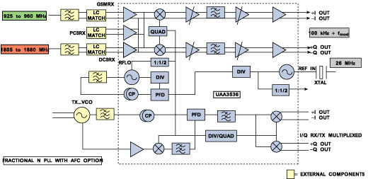
Cost-effectiveness is ensured through the highly integrated design of the IC, which, among its many on-chip features, includes a high dynamic range IF channel filter, a low noise amplifier (LNA) with image rejection front-end, fractional-N frequency synthesizers and a transmit offset loop with integrated filters. Its unique NZIF architecture offers better immunity to interference than ZIF solutions and also reduces RF development time. The UAA3536, which operates down to 2.6 V, interfaces with standard A/D converters and requires very few external components, simplifying circuit design problems and reducing component, assembly and logistics costs for handset manufacturers. All these innovative techniques offer a solution that reduces the PCB area by more than one third.
Key features demonstrating this new architecture's capabilities include a triple-band RF solution for GSM900/1800/1900 cellular phone systems, with integrated on-chip data services (GPRS Class 12 (4RX-4TX) with data rate up to 57.6kB/s and EDGE (4RX) with data rate up to 237kb/s). It has an integrated IF channel filter and integrated Tx low pass filters, with multi-band Tx modulation loop architecture including an offset mixer and a phase-frequency detector. The IC includes a fully integrated fractional-N RF synthesizer with AFC control capability and very fast switching time, along with a fully integrated RF VCO with integrated supply regulator and a semi-integrated reference oscillator with integrated supply regulator. The device operates down to 2.6 V and up to 3.6 V, and is housed in a new MLF package that offers 30 percent size reduction.
Conclusion
The innovative NZIF architecture allows the handset manufacturers to benefit from leading edge technologies. The highly integrated transceiver and baseband circuits will be a major step in preparing the way towards a dual mode GSM/UMTS handset, by having the GSM/GPRS/EDGE portion already optimized in performance, size and cost.
The different technologies presented here allow state-of-the-art product for 3G standards to be proposed. The cellular product evolution towards GSM/TDMA or any other multi-mode standards will need to concentrate most of the analog sensitive functions within the RF part and allow the digital part to integrate more and more memory with increased Mips requirements. This will lead to a different partitioning approach, offering many challenging tasks to the RF engineers. It is a first step towards a software radio.
Yvan Droinet is the international marketing manager of GSM RF standard products for Philips Semiconductors. In this position he is responsible for marketing Philips Semiconductors' wide range of cellular RF standard solutions worldwide. He has previously handled the position of development group leader. Before joining Philips Semiconductors, Mr. Droinet handled several positions in design and applications in different companies such as Dialog Semiconductors, Harris Semiconductors and Alcatel. He has built a broad technical expertise and was involved in the design of complex mixed analog/digital ASICs. Mr. Droinet studied electrical engineering at the 'Université Catholique' of Louvain-La-Neuve, Belgium. He is based in Caen, France.