

Next generation communication systems are requiring faster receiving, transmitting and handling of data loads. While those data loads are rapidly growing, power availability is not scaling at the same rate. Therefore, next generation and subsequent generation Transmit and Receive (Tx/Rx) modules need to handle more data while accommodating ever increasing power efficiency per bit. This will require a scalable technology solution with reduced form factor that allows closer integration with the antennas.
Traditional methods to achieve power and performance scaling to meet next generation needs have come from a combination of new architecture developments along with taking advantage of semiconductor node scaling. Since the inception of the integrated circuit, Moore’s Law has offered area and power scaling with each successive generation on an 18-24 month timescale that still continues to this day. Today, designers have access to semiconductor technology from standard CMOS to a multitude of III-V and II-VI materials that enables high speed digital, mixed signal and analog designs from DC to hundreds of GHz. However, implementation of a highly integrated solution presents many challenges.
- Lowest Common Technology Denominator: In order to meet performance specifications, all aspects of the die design must be designed on the highest performance technology node in order to minimize Size, Weight and Power (SWaP). This generally results in the longest schedules and the highest cost, as this is the most advanced node with the highest design complexity, NRE cost, mask costs and wafer costs. Today’s most advanced nodes have mask costs alone approaching $10 M. Hence it is not unreasonable to expect acquisition costs to exceed $30-$40 M for the most complex designs. Additionally, closure of these complex designs on first spin becomes more difficult, which will inevitably lead to additional mask set purchases to achieve acceptable performance.
- Mixed Technologies: Traditional board level designs have followed the monolithic package approach. The ability to leverage multiple and mixed technologies (Si CMOS, SiGe, GaAs, GaN, etc.) enable more efficient system designs. Approaches using monolithic ASIC solutions require the designer to select a single solution often requiring trade-offs in order to be implemented. As both digital and RF requirements continue to grow, multiple technologies will be required to deliver the full system performance.
- Yield: The push for System on Chip (SoC) to take full advantage of SWaP scaling is driving designs to larger footprints with higher levels of integration. Wafer fabrication manufacturers continue to improve clean room control, but yields are still defect density (and thus area) driven. This means that larger die will inherently produce lower yields, which in turn drives up cost.
- Scalability: Next generation capability in receive, transmit and data handling capability must be planned for. The technology solution for these systems should enable further scaling for power efficiency, increased channels and small form factors. SiP allows this by scaling individual components of the product versus an entire SoC revision.
There are multiple approaches to achieve SiP and HI, generally categorized into three broad topics:
- 3D: Stacking multiple active die on top of one another to achieve a fully integrated solution. This technique requires each die be designed to fit with the next die in the stack, and to create interconnects through the base substrate material (thru-wafer/die vias). 3D is seen as a potential future state but has not taken off except for the low power memory markets as getting heat out of the other more power hungry die within the stack has proven elusive.
- 2.5D: This involves the use of a silicon or glass interposer with vias to create extremely high density interconnects between multiple die. Silicon is readily available and advanced nodes can provide interconnect densities well below 2 µm in pitch. Cost, supply chain and product reliablity are all critical topics to determine if a 2.5D solution is the best choice. There are several high performance products on the market today from large commercial suppliers.
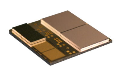
Figure 1: Cobham 2.5D Daisy Chain Reliability Demonstrator
- 2.1D: Using a high density organic interposer with 4-15µm pitch interconnects compomises the 2.1D solution. It’s essentially a high density MCM. Cost, performance, density and supply chain are integral factors to consider for a 2.1D approach. There are a multitude of 2.1D products on the commercial market today.
A final special consideration for microwafer products is moving from chip and wire to flip chip configurations, especially with III-V material sets.These wafers tend to be from 2" to 8” wafer diameters with thicknesses from 50-150 µm post fab and include thru-wafer vias as well as gold backside metalization.
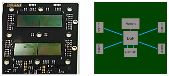
Figure 2: Cobham 2.1D Product Example (left) and Concept (right)
Wafer bumping of these thin wafers is challenging and has typically lead to stud bumping rather than traditional solder bumping.However stud bumping can be cost prohivitive and limits the potential future assembly processes. Cobham can provide solutions for stud bumping, solder bumping or copper pillar bumping of thin wafers.
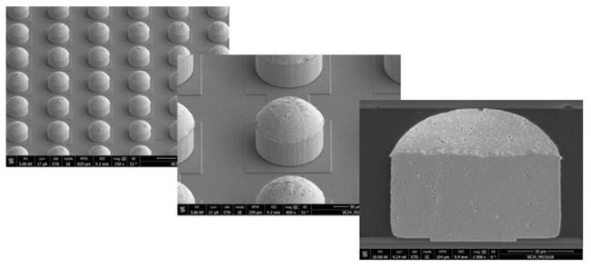
Figure 3: Cobham 150µm Pitch, Copper Pillar Bumping Example
Furthermore Cobham understands the performance vs reliabliity tradeoffs of protective coatings on the wafer as well as the underfill process.Planning for and modeling the appropriate assembly processes and materials leads to first pass success on both performance and reliablity. This reduces the overall cost of new products as well as speeds the time to market.
Cobham Advanced Electronic Solutions (CAES) is a provider of high reliabliaty-radiation hardened Application Specific Integated Circuits (ASICs), standard products, advanced packaging services and electronic manufacturing services for the defense and commercial space communities over the last 40 years. CAES’ business unit Semiconuctor and Space Solutions (SCSS) span the full range of military missions. Cobham Advanced Pacaging Solutions (CAPS) offers the Hetrrogeneous Intgration (HI) of multiple and mixed technologies (Si CMOS, SiGe, GaAs, GaN, etc.) and System-in-Pacakging (SiP) that is availble for our customers. Our Cat 1A Trusted Manufacturing and Design center is located in Colorado Spring, CO and includes a facility with over 5,000 sqft of QML cerrified class-100 clean room space. Our development and design teams have brought over 1000 products to market and have been the leaders in new technology development and adoption across the community.