
Analog Devices has developed a pair of highly integrated up-converter (ADMV1013) and down-converter (ADMV1014) ICs covering 24 to 44 GHz with greater than 1 GHz instantaneous bandwidth. Matched to 50 Ω, the ADMV1013 and ADMV1014 simplify the design and implementation of mmWave platforms for the popular 28 and 39 GHz 5G bands, whether backhaul, fronthaul or other wide bandwidth transmitter and receiver applications.
The up- and down-converter ICs are highly integrated (see Figure 1), comprising I/Q mixers with on-chip quadrature phase shifters. The converters are configurable for direct conversion to or from baseband (DC to 6 GHz) or an IF (800 MHz to 6 GHz). The up-converter RF output has an on-chip driver amplifier with a voltage variable attenuator (VVA), while the down-converter’s RF input starts with a low noise amplifier (LNA), followed by a VVA and gain stage. Each local oscillator (LO) chain contains an integrated LO buffer, frequency quadrupler and programmable bandpass filter. Most of the programmability and calibration are controlled with a serial peripheral interface (SPI), making the ICs easily configurable via software.
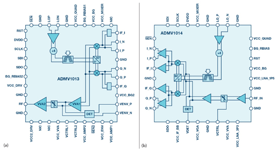
Figure 1 Block diagrams of the ADMV1013 up-converter (a) and ADMV1014 down-converter (b).
ADMV1013 UP-CONVERTER
The ADMV1013 has two modes of frequency translation: direct from baseband and single sideband up-conversion from IF. With direct up-conversion, the baseband I and Q differential inputs accept signals from DC to 6 GHz and are compatible with high speed digital-to-analog converters (DAC). The inputs have a configurable common-mode range from 0 to 2.6 V, which accommodates the interface requirements of most DACs, simplifying the interface design. The second mode is typically for signals generated by a quadrature digital up-converter.
Unique to the ADMV1013 is the capability to allow digital correction of the I and Q mixers’ DC offset error in the I/Q mode, which reduces the LO leakage to the RF output. After calibration, the LO leakage can be as low as −45 dBm at the RF output at maximum gain. An even more difficult challenge that plagues direct conversion radio design is I/Q phase imbalance, which causes poor sideband suppression. An added challenge with direct conversion: the sideband is usually too close to the microwave carrier, making filtering impractical. The ADMV1013 solves this problem by enabling users to digitally correct for the I/Q phase imbalance with register tuning. In normal operation, the up-converter exhibits an uncalibrated sideband suppression of 26 dBc. Using the on-chip registers, the sideband suppression after calibration can be improved to about 36 dBc. Both correction features are accessed via the SPI and do not require extra circuitry. Additional suppression can be achieved in the I/Q mode by adjusting the phase balance of the I and Q baseband DACs. These performance capabilities improve microwave radio performance while minimizing external filtering.
With the LO buffer amplifier integrated on-chip, the up-converter only requires 0 dBm drive, enabling the IC to be driven directly from a synthesizer with an integrated voltage-controlled oscillator (VCO), such as the ADF4372 or ADF5610, reducing the external components. The on-chip frequency quadrupler multiplies the LO frequency to the desired carrier frequency, and the signal is passed through a programmable bandpass filter to reduce the undesired multiplier harmonics, prior to feeding the mixers’ quadrature phase generator stage. This reduces spurious injection into the mixers and allows the IC to work with an external low cost and low frequency synthesizer or VCO.
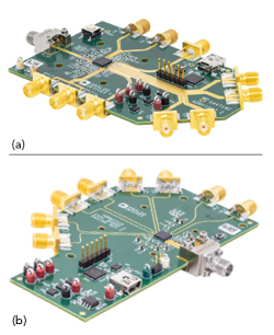
Figure 2 Evaluation boards showing the 6 mm x 6 mm surface-mount ADMV1013 up-converter (a) and 5 mm x 5 mm ADMV1014 down-converter (b).
The modulated RF output from the mixer is amplified through a pair of amplifier stages with a VVA between them, providing an adjustable gain range of 35 dB and a maximum cascaded conversion gain of 23 dB. The ADMV1013 is packaged in a 6 mm x 6 mm, 40-pin land grid array (see Figure 2a).
ADMV1014 DOWN-CONVERTER
Similar to the up-converter, the ADMV1014 has the LO buffer, frequency quadrupler, programmable bandpass filter and quadrature phase shifter in the LO path. However, as a down-converter, the ADMV1014’s RF signal chain has an LNA followed by a VVA and amplifier (see Figure 1b). Controlled by a DC voltage applied to the VCTRL pin, the down-converter’s gain has a continuous adjustment range of 19 dB.
The ADMV1014 also has two modes of frequency translation: direct down-conversion and as an image-reject down-converter to single-ended I and Q IF ports. Configured as a direct conversion demodulator from microwave to baseband, the demodulated I and Q signals are amplified at the respective differential outputs, with the gain and DC common-mode voltage set by registers via the SPI. This enables the output to be DC coupled to a pair of baseband analog-to-digital converters (ADC). In either mode, the I and Q phase and amplitude imbalance can be corrected via the SPI, improving the down-converter’s image rejection whether it demodulates to baseband or IF.
Overall, the down-converter provides a cascaded noise figure of 5.5 dB with a maximum conversion gain of 17 dB from 24 to 42 GHz. Near the band edge of 44 GHz, the cascaded noise figure remains respectable: 6 dB. The ADMV1014 is slightly smaller than the up-converter IC, measuring 5 mm x 5 mm (see Figure 2b).
BOOSTING RADIO PERFORMANCE
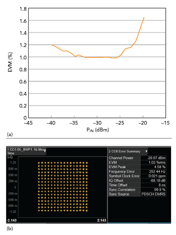
Figure 3 Measured RMS EVM vs. input power (a) and corresponding 256-QAM constellation (b) of the down-converter at 28 GHz.
Figure 3 shows the measured performance of the down-converter at 28 GHz with a 5G NR 256-QAM waveform composite of four independent 100 MHz channels at −20 dBm input power per channel. The resulting error vector magnitude (EVM) measured −40 dB (1 percent RMS), which supports demodulating the higher-order modulation that mmWave 5G systems require.
With greater than 1 GHz bandwidth and 23 dBm output third-order intercept (OIP3) for the up-converter and 0 dBm input IP3 for the down-converter, the two devices support high-order QAM, enabling high data throughput. These capabilities offer designers flexibility and ease of design, while requiring minimal external components. The small size combined with high linearity and image rejection are compelling, supporting high performance and small form factor microwave links and broadband base stations. In addition to 5G, the up- and down-converters will serve applications such as satellite and Earth station broadband communication links, secured communication radios, RF test equipment and radar systems.
Analog Devices
Norwood, Mass.
www.analog.com