
In a recent head-to-head test, defense contractor Harris Corp. created 3D printed RF amplifier and antenna circuits and compared them with the same designs fabricated with traditional printed circuit board (PCB) methods. Both circuits printed by additive manufacturing worked just as well as those created using traditional PCB manufacturing and were printed days faster than with the conventional method. This demonstration was intended to show the feasibility of precision 3D printed electronics for defense and aerospace applications.
Engineers at Harris partnered with Nano Dimension, a manufacturer of 3D printers for printed electronics, to see how RF circuits created with additive manufacturing (3D printing) compare with those made using conventional manufacturing processes. The study comprised circuit design and simulation, fabrication and testing. The goals set by the Harris team were to study the use of 3D printing for functional RF circuits by demonstrating how the 3D printed circuits compare with those made by conventional manufacturing. The proof-of-concept test vehicles were a 2 GHz amplifier and an RF antenna designed to operate at 5.2 GHz. The details and experimental results of the study follow, with a discussion of the implications for RF manufacturing.
From the ocean to orbit, Harris provides mission-critical systems to connect, inform and protect the world. The company is a leader in tactical communications, EW, avionics, air traffic management, space and intelligence and weather solutions. Developing circuits and systems for conveying data, video and voice across long distances, Harris has focused on improving system mobility and performance while working to reduce development time and cost - particularly important for complex defense and space systems. Hence, the company’s interest in additive manufacturing.
This study on using additive manufacturing to develop RF circuits for wireless systems is part of a joint project with the Israel Innovation Authority and Space Florida Foundation, a partnership promoting research, development and the commercialization of aerospace and technology projects. In June 2017, Nano Dimension received an Israel Innovation Authority grant to collaborate with Harris to apply 3D printing to electronic modules. The project was designed to demonstrate 3D printing of double-sided, multilayer circuits integrating digital, power and RF signals could reduce the SWaP-C of space systems.
Building the RF Circuit
Creating RF components for complex systems is typically a complex, multi-stage process. Achieving the optimum component and system performance is iterative: create a design, produce a prototype circuit, test its performance to identify shortfalls, change the design, build and test another prototype and repeat until the optimum design is achieved. This process has long lead times and is expensive. With electronic components the heart of automotive, defense, consumer and medical devices, the capability of 3D printing to prototype PCBs and other components in just hours and onsite - regardless of the circuit’s complexity - yields time and cost savings and supports rapid innovation.
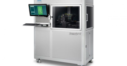
Figure 1 DragonFly 3D printer.
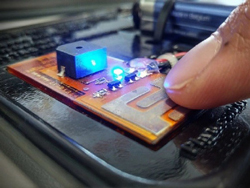
Figure 2 Phytec touch sensor printed with the DragonFly 3D printer.
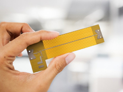
Figure 3 3D printed RF amplifier using the DragonFly Pro system.
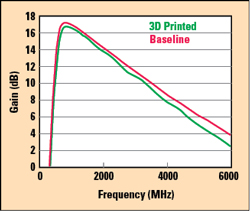
Figure 4 Gain of the 3D printed and conventionally manufactured amplifiers.
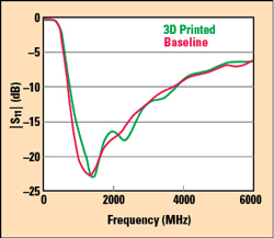
Figure 5 |S11| of the 3D printed and conventionally manufactured amplifiers.
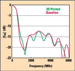
Figure 6 |S22| of the 3D printed and conventionally manufactured amplifiers.
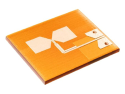
Figure 7 Nano Dimension 3D printed 5G antenna.
To fabricate the 3D printed circuits for this study, Harris used Nano Dimension’s DragonFly printer (see Figure 1), the first commercial additive manufacturing system for printed electronics. DragonFly provides essentially unlimited possibilities for creating densely packed electronic prototypes and rapid design iterations. The high-resolution system prints metal and polymer simultaneously, for PCBs and precision electronics such as sensors, RF circuits, antennas, molded interconnects and customized parts such as smart cards, RFID circuits and other ID products and arrays (see Figure 2). With the DragonFly, circuits and systems that have rigid packaging integrated with flexible circuits can be produced in a single print, without the need for cables and connectors.
Harris selected Nano Dimension because the DragonFly 3D printer is designed to drastically reduce development time and cost, while enabling the fabrication of complex electronic systems that cannot be manufactured by conventional means. The printer uses conductive silver and dielectric inks tailored for use in 3D printed electronics. To assess the applicability of 3D printing for RF systems, Harris designed, simulated and tested a 3D printed RF amplifier and compared it with an amplifier fabricated using conventional manufacturing of a PCB using an FR4 substrate. Both the amplifier and antenna were designed using electromagnetic simulation software. Once the beam and radiation patterns of the antenna were simulated and set, the file was converted and uploaded to the DragonFly for 3D printing. The resulting circuit fabrication matched the original design nearly identically, demonstrating the expected functionality.
The RF amplifier (see Figure 3) was built by Harris in a single print, with the fabrication taking about 10 hours using Nano Dimension’s silver nanoparticle conductive and dielectric inks. Components were manually soldered to the PCB, which measured 101 mm x 38 mm x 3 mm. The traditionally manufactured circuits, in contrast, were sent to a prototyping facility to be manufactured, a process with cycle times that typically take days to weeks. The amplifier printed using the DragonFly was designed for 2 GHz and performed close to the simulation out to 6 GHz. The frequency response was higher than anticipated and comparable to amplifiers fabricated on FR4 substrates using conventional PCB manufacturing steps.
Test Results
To assess the quality of the 3D printed RF circuit versus traditional PCBs, Harris measured small signal gain, input return loss and output return loss for each amplifier. Harris engineers determined the RF circuits printed with additive manufacturing performed the same as those fabricated using traditional methods, demonstrating the viability of 3D printing technology to produce functional RF circuits.
Figure 4 compares the gain of the 3D printed and conventional amplifiers, showing less than 1 dB difference to 4700 MHz and less than 1.3 dB to 6000 MHz. The lower gain with the 3D printed amplifier was attributed to higher losses in the dielectric and metal transmission lines. Figure 5 compares the |S11| of the two prototypes, showing no material difference in the responses of the amplifiers from 10 MHz to 6000 MHz. Similarly, the |S22| of the two, shown in Figure 6, reflects essentially the same responses over frequency. Harris presented these results and conclusions at the 2019 IEEE Radio & Wireless conference in Orlando.1
Given these performance results and the capability to rapidly and affordably manufacture prototypes, Harris plans to further develop 3D printing technology, including tests in actual field environments such as space. In addition to land-based reliability testing, hardware developed by Harris using the DragonFly will fly on the International Space Station, where it will be tested for communications capabilities with Harris’ satellite tracking station in Florida. This project will provide a systematic analysis of 3D printed materials for space systems, which is especially applicable for nano-satellites.
Implications for Aerospace and Defense
The results of this study are a significant milestone for the additive manufacturing of electronics in a variety of industries, including aerospace and defense. They demonstrate the viability of 3D printed electronics for RF circuits, showing the potential to play an important role advancing the small satellite and low Earth orbit (LEO) constellations. These satellites have many possible uses, from broadband internet access to IoT networks. 3D printing technology can play critical roles in nearly every aspect of research, design and manufacturing, offering significant advantages such as performance, rapid development and the ability to print complex shapes not achievable using traditional manufacturing processes.
Harris and Nano Dimension plan to improve the high frequency performance of the 3D printed circuits, as well as fabricating more compact and denser circuitry. The capability to rethink circuit design - even considering flexible substrates and uniquely shaped circuits - is a major benefit of additive manufacturing, as it can create shapes not feasible using traditional fabrication.
Summary
3D printed electronics offers a range of benefits: The capability to 3D print RF electronics and antennas in house significantly reduces the time and cost of prototyping and proving new concepts. Being able to 3D print antennas with similar performance to traditional antennas can be a catalyst for rapid advancements in radio communications (see Figure 7). 3D printing enables even smaller and lighter antennas with rigid packaging integrated with flexible circuits, eliminating cables and connectors. Beyond reducing cost and cycle time and offering more flexible production, the capability reduces intellectual property risk.
Reference
- A. C. Paolella, “Directions in 3-D Printed RF Systems for Space Applications,” 2019 IEEE Radio & Wireless Week, Melbourne, Fla.