
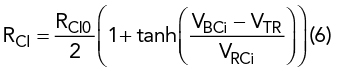
Figure 2 Measured vs. modeled forward (a) and reverse (b) Gummel plots.
where VTR, RCI0 and VRCi are three fitting parameters. At the transition voltage, VBCi = VTR, the intrinsic collector resistance takes on half of the value RCI0 needed to fit the knee region of the IC-VCE characteristics. The parameter VRCi controls the steepness of the transition from RCI0 to zero.
The high frequency performance is defined by a charge model; therefore, the AC characteristics include depletion charge and diffusion charge. The depletion charge for both the base-emitter and base-collector junctions is based on the Keysight HBT model, where the depletion charge functions for both the base-emitter and base-collector junctions are based on the formulation from HICUM (version 2.1). This formulation and its derivatives are fully continuous for all regions of bias, appropriate for a large-signal computer-aided design model.
MODEL VERIFICATION AND DISCUSSION
The present compact empirical large-signal model has been applied to various sized InP HBT transistors; with limited space, only the 1 x 15 μm2 emitter area transistor is discussed in this article. The parameter extraction procedure starts by extracting the access resistors using the open collector method.6-7 Second, the DC parameters are extracted from forward and reverse Gummel plots using a semiconductor parameter analyzer. Third, the small-signal model parameters are extracted from a large number of small-signal S-parameters at multiple bias points.
To verify the model, DC and small-signal characteristics were measured at multiple bias points. The measured data was obtained on-wafer with a Keysight B1500A semiconductor device analyzer for DC parameters and an HP8510C network analyzer for small-signal S-parameters, across the range from 0.1 to 40 GHz. The measurements were performed after the substrate was thinned to 100 μm and the backside gold-electroplated.
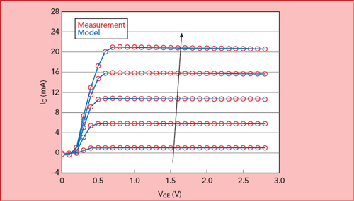
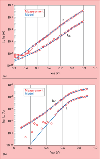
Figure 3 Modeled vs. measured IC-VCE. IB is from 20 to 340 μA in steps of 80 μA.
Figure 4 Modeled vs. measured S11 (a), S12 (b), S21 (c) and S22 (d) with IC = 1, 11 and 21 mA and VCE = 1.7 V.
The forward and reverse Gummel plots are shown in Figure 2, comparing measured and simulated, and Figure 3 plots the IC-VCE curve comparison. In addition to the output DC IC-VCE and Gummel characteristics, the model was validated by comparing measured and simulated S-parameters over a range of collector currents, from 1 to 21 mA, and from 0.1 to 40 GHz. Figure 4 shows the S-parameter fit for IC from 1 to 21 mA and VCE = 1.7 V. The model versus measured S21 shows some deviation at low current and low frequency. As the model is formulated on a certain region for a special application, in this work, the main interest is in the operating region where IC = 11 mA; the model shows a better fit in this region.
CONCLUSION
A nonlinear circuit simulation model for InP DHBTs based on a charge formulation and an accurate large-signal model has been implemented using a seven-port SDD in Keysight ADS. The model is flexibly modified due to the equation-based SDD component and accounts for self-heating and soft knee effects. Good agreement between measured data and simulation was achieved.
ACKNOWLEDGMENT
This work was supported by the National Natural Science Foundation of China (Grants 61804046, 61704049), the Doctoral Scientific Research Foundation of Henan University of Science and Technology (Grant 400613480011) and the Foundation of Department of Science and Technology of Henan Province (Grants 172102210258, 182102210295).
References
- J. C. Zhang, B. Liu, L. M. Zhang, L. Sun, J. Wang and L. Song, “A Rigorous Peeling Algorithm for Direct Parameter Extraction Procedure of HBT Small-Signal Equivalent Circuit,” Analog Integrated Circuits and Signal Processing, Vol. 85, No. 3, June 2015, pp. 405-411.
- C. Rehorn, “InP HBT Chipset, Enabling High-Bandwidth, Real-Time Oscilloscope Architecture,” Microwave Journal, Vol. 53, No. 7, July 2010.
- M. Schröter, T. Nardmann and G. Wedel, “A Closed-Form Solution for the Low-Current Collector Transit Time in Group IV and Group III-V HBTs,” IEEE Transactions on Electron Devices, Vol. 64, No. 8, August 2017, pp. 3346-3352.
- A. Bennour, Z. G. Tegegne, S. Mazer, J. L. Polleux, M. El Bekkali and C. Algani, “Large-Signal Static Compact Circuit Model of SiGe Heterojunction Bipolar Phototransistors: Effect of the Distributed Nature of Currents,” IEEE Transactions on Electron Devices, Vol. 65, No. 3, March 2018, pp. 1029-1035.
- T. K. Johansen, V. Midili, M. Squartecchia, V. Zhurbenko, V. Nodjiadjim, J. Y. Dupuy, M. Riet and A. Konczykowska, “Large-Signal Modeling of Multi-Finger InP DHBT Devices at Millimeter-Wave Frequencies,” International Workshop on Integrated Nonlinear Microwave and mmWave Circuits, April 2017.
- J. Gao, X. Li, H. Wang and G. Boeck, “Approach for Determination of Extrinsic Resistance for Equivalent Circuit Model of Metamorphic InP/InGaAs HBTs,” IEEE Proceedings Microwaves, Antennas and Propagation, Vol. 152, No. 3, September 2005, pp. 195-200.
- J. Krause and M. Schröter, “Methods for Determining the Emitter Resistance in SiGe HBTs: A Review and an Evaluation Across Technology Generations,” IEEE Transactions on Electron Devices, Vol. 62, No. 5, May 2015, pp. 1363-1374.