
Carbon nanotube (CNT) transistor technology has intrinsic linearity due to its ballistic transport properties and is CMOS compatible for monolithic integration.
RF environments are becoming ever more crowded with unwanted RF signals entering the broadband RF front-end amplifier, resulting in receiver-generated third-order intermodulation distortion (IMD3) products. By their nature, IMD3 products often fall near the frequencies that the receiver is tuned to and are generally difficult to filter. Consequently, receiver-generated IMD3 products can swamp weak desired signals and, when present in large numbers, form an effective noise floor that exceeds the noise floor from the receiver noise figure, reducing dynamic range. In digital communications, the resulting reduced sensitivity shows up as an increased bit error rate (BER) that limits range and data transfer speed. As such, a higher amplifier output third-order intercept point (OIP3) is desirable, because for each dB increase in OIP3, IMD3 levels fall 2 dB for a given fundamental signal power. While increasing transistor size and DC bias power can increase OIP3, many systems - satellites and mobile/portable devices - face restrictive power budgets. OIP3 can also be increased with circuit-based linearization; however, these perform worse as frequency increases. For a given circuit approach, the OIP3 improvement can still benefit from improvements in the underlying transistor technology. It is more desirable to fundamentally improve the transistor intrinsic linearity than to rely exclusively on the above approaches.1
A transistor’s intrinsic linearity transfer curve, i.e. drain current (Id) versus gate voltage (Vgs), can be represented by its linearity figure of merit: OIP3/Pdc in dB, where Pdc is the DC bias power consumption. Newer and denser modulation schemes, such as 256-QAM for 5G, demand RF front-ends with high OIP3/Pdc ratios for high sensitivity and band use efficiency, combined with low power use. Military battlefields are signal-rich and require high OIP3/Pdc ratios1 for high dynamic range and sensitivity, combined with long battery life.
Owing to the maturity of present semiconductors, it is likely that new, truly disruptive improvements in OIP3/Pdc or frequency performance will require a rethinking of potential RF semiconductor device materials and structures beyond incumbent technologies. In the interest of cost control and scalability to monolithic integration, the new device structures must also be CMOS compatible.
One technology is CNT field-effect transistors (CNT-FET) fabricated from aligned semiconducting CNTs, which operate via one-dimensional carrier transport. Since their discovery in 1991, these ~1.5 nm cylindrical molecules of carbon have been talked about as an emerging high performance electrical material. Although CNTs have long been known to have impressive transport properties, such as high current and transconductance exceeding 25 μA and 20 μs per tube, for much of that time the twin engineering challenges of achieving high purity semiconducting CNTs (> 99.9 percent) and dense, aligned arrays (> 40 CNTs/μm) have prevented the full manifestation of these properties in a practical device. Now, these challenges have been overcome to improve device performance.
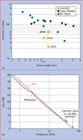
Figure 1 Comparison of Carbonics CNT-FET4-5 ft vs. GaAs PHEMT and RF CMOS technologies (a). A 110 nm gate length CNT-FET fabricated in 2018 achieved an extrinsic ft of 60 GHz (b).
These devices offer intrinsically superior transfer curve linearity and, therefore, higher OIP3/Pdc ratios compared to incumbent semiconductor devices.2 CNT transistor technology developed by Carbonics combines the intrinsic linearity advantages of CNT electronic transport properties with an approach that has been shown to both theoretically2 and empirically3 maximize OIP3/Pdc. CNT-FET technology has achieved new records for ft (see Figure 1), increasing from 22 GHz in 2015 to 60 GHz in 2018, and Carbonics’ CNT-FETs have achieved an OIP3/Pdc of 15.7 dB, and an OIP3 of 11.5 dBm. Low voltage operation (< 3 V) and CMOS compatibility provide a path to monolithic integration of the digital and analog worlds.
CNT-FET SPECIFICATIONS AND ON-WAFER MEASUREMENTS
As a proof of feasibility beyond on-wafer measurements, two L-Band amplifiers (amplifiers 1 and 2) have been built and demonstrated. The CNTs have molecular structures similar to graphene (i.e., hexagons of carbon atoms), except that they are formed into tubes and the direction of the rollup (i.e., the chirality vector) determines their electronic properties.6 Some chiralities have zero bandgaps (i.e., metallic) and others have non-zero bandgaps (i.e., semiconducting CNTs).
Present CNT production processes cannot control chirality. Hence, approximately one third of the as-grown CNTs are metallic, with the remainder semiconducting. Only the semiconducting CNTs are useful for CNT-FETs because the current in metallic CNTs cannot be modulated by electric fields through an insulator, required to construct a useful field-effect transistor. CNTs used for CNT-FETs must be sorted to remove those that are metallic.
The CNT-FETs in this work are constructed from high purity semiconducting CNTs having a very small fraction of metallic CNTs, on the order of 0.1 percent. This ensures minimal transistor leakage current. These are then deposited as a monolayer on a quartz wafer using Carbonics’ proprietary ZEBRA wafer deposition process, producing the CNT monolayer shown in Figure 2a. The CNT-FETs used in both amplifiers have gate widths of 50 μm and gate lengths of 140 nm. Figure 2b shows a CNT-FET, similar to those used in the amplifiers, fabricated on a quartz substrate. The CNT-FETs used in the amplifiers come from wafers with on-wafer measurements showing extrinsic fmax and ft reaching up to 60 GHz and 43 to 60 GHz, respectively, at Vds = −1.5 V. CNT-FETs used in amplifiers 1 and 2 have maximum drain currents, Idmax, of 143 mA/mm and 228 mA/mm, respectively, with on/off ratios at Vds= −1 V of 233 and 121, respectively, which indicates a very low metallic CNT fraction.
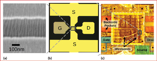
Figure 2 SEM image of an aligned monolayer of high purity semiconducting carbon nanotubes spanning the FET channel prior to forming the T-gate (a), CNT-FET (b) and CNT-FET die mounted on an alumina chip carrier (c).
DEVICE, CHIP CARRIER AND AMPLIFIER STRUCTURE
The quartz substrate CNT-FETs are diced and selected for mounting to alumina chip carriers as shown in Figure 2c. The hard alumina chip carriers accommodate wire bonding while enabling softer, low loss RF material to be used for the RF printed circuit boards (PCB). Laser fabrication tools are employed to fabricate and pattern the metallization of the 254 μm thick alumina chip carriers, steps conducted at the University of California, Los Angeles Center for High Frequency Electronics (UCLA CHFE). This technique enables the formation of excavated pockets behind the pads to reduce parasitic capacitance. The chip carrier design includes probe pad structures to allow wafer probes to directly measure the S-parameters of the mounted CNT-FET while automatically including the RF characteristics of the die to chip carrier bond wires. After mounting, the CNT-FET chip carriers are probed on the chip carrier pads, enabling accurate design of the RF amplifier PCB’s impedance-matching and bias structures without needing to model the carrier.
Amplifier 1’s CNT-FET, mounted on the chip carrier, demonstrated an ft and fmax of 3 and 7.9 GHz, respectively, while amplifier 2’s CNT-FET measured 5 and 8 GHz. The large decrease from the measured on-wafer ft and fmax is likely due to bond wire parasitic inductance and resistance. At 1.2 GHz, the maximum stable gain (MSG) for amplifiers 1 and 2 wire bonded in the chip carriers is 16 and 17 dB, respectively.
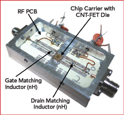
Figure 3 Packaged CNT-FET amplifier.
NI AWR Microwave Office® is used to design the amplifier input and output matching circuits to achieve maximum gain near 1.2 GHz. The selected CNT-FETs’ small gate peripheries result in very small input capacitances < 0.6 pF, which results in high capacitive gate impedances of approximately 220 Ω at 1.2 GHz. This necessitates matching gate inductances on the order of 31 nH. Under such conditions, the use of lumped elements saves space and yields higher Q and gain than possible with microstrip elements alone.
The microstrip tuning and bias network elements are etched onto a Rogers R04350B RF substrate. Passive components are bonded on the PCBs using conductive epoxy. The PCBs are then glued into their aluminum housings and connectors added. Finally, alumina chip carriers, containing the CNT-FETs are mounted using conductive epoxy and the electrical connections are made using wires attached with conductive epoxy (see Figure 3).
MEASUREMENT RESULTS AND DISCUSSION
Gain, return loss, OIP3 and 1 dB gain compression were measured with a scalar analyzer. At Vds = −1.16 V and Vgs = −1.1 V, amplifier 1 produced a peak gain of 11.6 dB, while the peak gain of amplifier 2 was 10 dB (see Figure 4). For amplifier 1, the gain was 4.4 dB below its MSG, while amplifier 2’s gain was 7 dB below its MSG. Amplifier 2’s gain, |S11| and |S22| responses versus frequency were similar to those of amplifier 1.
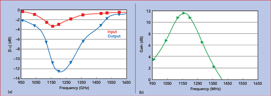
Figure 4 Input and output |S11| (a) and gain (b) of amplifier 1.
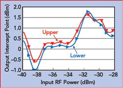
Figure 5 Amplifier 1 OIP3 with 1160 and 1171 MHz input tones.
OIP3 was measured by applying two RF signals at 1149 and 1182 MHz. The two OIP3 values - the lower and upper frequency IMD3 products - are plotted in Figure 5 for amplifier 1. Amplifier 1’s OIP3 ranged from −1 to +1.8 dBm. For comparison, amplifier 2’s OIP3 was from −1.8 to +0.4 dBm. The measured 1 dB compression point for amplifier 1 was −10.3 dBm (see Figure 6), while the 1 dB output compression point for amplifier 2 was −11.9 dBm. This implies OIP3 to P1dB differences of approximately 10 and 12 dB for amplifiers 1 and 2, respectively, which meets or exceeds the 10 dB rule of thumb for most semiconductor devices.
Overall, these results go beyond the work by Eron et al.7 who demonstrated an L-Band CNT-FET amplifier fabricated from CVD-grown CNTs. However, that CNT-FET5 had significant metallic CNT content and, consequently, relatively high leakage current compared to the CNT-FETs discussed here.
FUTURE DIRECTIONS AND POTENTIAL
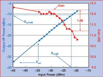
Figure 6 Amplifier 1 output power and gain vs. input power, measured at ~1.2 GHz.
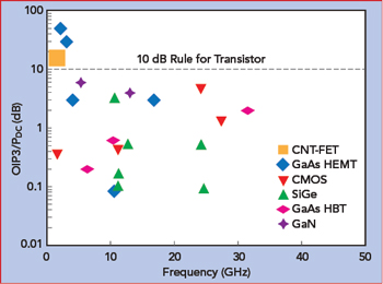
Figure 7 Linearity comparison of 2018 CNT-FET vs. incumbent process technologies.1 Here, the CNT-FET OIP3/Pdc = 15.7 dBm at 1.5 GHz.
The empirical results achieved and described in this article demonstrate the capability of CNT-FET technology employing aligned CNT ZEBRA wafers. In this circuit design, however, the die was designed for optimal wafer probing; consequently, the large die requires long bond wires, on the order of 2 mm, which is the primary performance limitation. A new mask set and redesign of the chip carrier should improve the performance of subsequent CNT-FET circuits; much-improved frequency response, lower noise figure and higher OIP3 are expected. Additionally, the CNT-FETs used in these amplifiers are mid-2018 iterations. More recent CNT-FETs fabricated in January 2019 benefit from the technology’s rapid trajectory since this first amplifier project and their results, to be published, show ft and fmax performance that already approaches that of GaAs PHEMTs and compares favorably to RF CMOS (see Figure 1), while also having the advantage of being compatible with CMOS. Rough projections based on single-tube measurements puts the upper range of CNT-FET device performance at transconductance values of 1200 μs/μm, current densities of 1500 μA/μm and ft around 300 GHz for 100 nm gate-length devices. Consequently, there is substantial headroom for continued advancement of the CNT-FET technology.
These latest CNT-FET OIP3 and OIP3/Pdc on-wafer results already compare favorably to CMOS and other technologies1 (see Figure 7). Carbonics sees CNT RF technology entering commercialization with discrete and MMIC products for the defense and aerospace markets within the next two to five years. It is suitable for highly sensitive front-end signal processing of high frequency signals used in radar, communications and other military systems, particularly well-suited for front-end modules and circuits such as mixers, oscillators, low noise amplifiers and power amplifiers. As the technology matures, more complex products and monolithic integration with CMOS are envisioned.
References
- “Dynamic Range-Enhanced Electronics and Materials (DREaM),” DARPA Broad Area Announcement, March 28, 2017.
- J. Baumgardner, A. Pesetski, J. Murduck, J. Przybysz, J. Adam and H. Zhang, “Inherent Linearity in Carbon Nanotube Field-Effect Transistors,”Applied Physics Letters, Vol. 91, No. 5, August 2007, pp. 052107–052107-3.
- S. Maas, “Linearity and Dynamic Range of Carbon Nanotube Field-Effect Transistors,” IEEE MTT-S International Microwave Symposium, June 2017.
- Y. Cao, G. J. Brady, H. Gui, C. Rutherglen, M. S. Arnold and C. Zhou, “Radio Frequency Transistors Using Aligned Semiconducting Carbon Nanotubes with Current-Gain Cutoff Frequency and Maximum Oscillation Frequency Simultaneously Greater than 70 GHz,” ACS Nano, Vol. 10, No. 7, June 2016, pp. 6782–6790.
- Y. Cao, Y. Che, H. Gui, X. Cao and C. Zhou, “Radio Frequency Transistors Based on Ultra-High Purity Semiconducting Carbon Nanotubes with Superior Extrinsic Maximum Oscillation Frequency,” Nano Research, Vol. 9, No. 2, February 2016, pp. 363–371.
- R. Caldwell, “Synthesis and Electronic Transport in Single-Walled Carbon Nanotubes of Known Chirality,” Ph.D. Thesis, Columbia University, 2011.
- M. Eron, S. Lin, D. Wang, M. Schroter and P. Kempf, “L-Band Carbon Nanotube Transistor Amplifier,” Electronics Letters, Vol. 47, No. 4, February 2011.