
Few technology applications are positioned to benefit from high-power RF GaN device insertion to the extent as space payloads. Costing roughly $10,000 per pound of payload to launch a satellite into space, the benefit of small, lightweight hardware is obvious. The trend toward low Earth orbit (LEO) satellite constellations is increasing the pressure to develop cost-saving technologies. While GaN is well-positioned to deliver these benefits, its use is not without challenges. To maximize the mean time between failures (MTBF), the thermal conduction path away from the device must be carefully designed. As an added challenge, the lack of industry heritage using GaN in space requires thorough analysis and additional qualification testing.
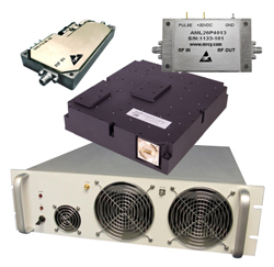
Figure 1 Increasingly used in radar, EW and communications application, GaN power amplifiers offer size, weight and power benefits for satellites.
GaN is a III-V direct bandgap semiconductor. Similar to GaAs, its high electron mobility makes it well-suited for RF/microwave applications. Compared to GaAs, the wider bandgap of GaN - 3.4 vs. 1.4 eV for GaAs - enables operation at very high-power densities. Instead of using bulky combining networks to sum the power of many GaAs devices, a small number of GaN devices will efficiently produce high output power. As GaN technology continues to mature (see Figure 1), it is replacing some traveling wave tube (TWT) amplifiers, which have been the primary technology for satellite power amplifiers for years.
SATELLITE AMPLIFIER TECHNOLOGY
As with nearly all communications systems, satellite transponders include transmit and receive modules. In the traditional architecture, the uplink signal is passed through a low noise amplifier to a frequency converter, then to the transmit module. Amplifying the signal to the required output level is typically the role of a TWT amplifier. While tube amplifiers produce high-power at Ka-Band, their large size and high-cost are challenging, especially evident with the new generation of LEO satellites. Since these satellites must be smaller and less expensive than traditional satellites, relying on expensive and large TWT amplifiers is problematic.
TWTs amplify RF signals through the interaction between an electron beam and the RF signal. While this is an efficient method for generating high output power, TWT amplifiers are inherently complex assemblies, requiring the mechanical integration of multiple, high-precision components. This complexity drives the high price of TWTs and increases the risk of failure. TWT amplifiers also require very high bias voltage - usually thousands of volts - generated by a high voltage supply, which is also large and expensive. As a rough order-of-magnitude, the size of a Ka-Band TWT amplifier with 500 W output power is about 18 in. x 3 in. x 3 in., with an equally large power supply. Not only does the large size of the TWT amplifier restrict its use in LEO satellites, even traditional satellites have strict size and weight limits on their payload systems and will benefit from smaller components.
A solid-state solution offers a more robust, compact option. A GaN power amplifier uses standard IC manufacturing processes, producing small devices only a few millimeters on each side. Instead of using artisan-style manufacturing, GaN devices are produced using automated semiconductor processes at low-cost. While a single GaN device is unable to deliver the same output power as a TWT amplifier, multiple GaN devices can be combined in a small package. As an added benefit, GaN amplifiers only require bias voltages of 28 to 50 V.
Given the differences between GaN and TWT amplifiers, GaN is particularly attractive for applications sensitive to size, weight and cost, as well as those that require less transmit power. This precisely describes LEO satellites.
CHALLENGES OF GaN IN SPACE
While GaN amplifiers offer compelling benefits for satellite applications, specific challenges must be overcome to successfully use GaN in space-qualified hardware. The first and most obvious challenge arises from the high power density of the device. While TWT amplifiers also require a complex cooling system, a GaN IC generates significant heat in a very small space. For example, a 30 W solid-state GaN amplifier can easily draw 2.5 A biased at 28 V, resulting in 40 W power dissipation in an area not much larger than 10 mm2. If the thermal transfer is inadequate to cool the device, the elevated junction temperature will lower output power and reduce MTBF - possibly even causing catastrophic failure.
This raises the second challenge: reliability. The high-power dissipation common with GaN devices results in a significant temperature rise in the active region; as the temperature in the device increases, the reliability of the amplifier degrades. The temperature rise depends on the power dissipation in the GaN and the thermal resistance between the device and the case - both difficult to model and control. Power dissipation depends on multiple factors such as RF drive and load impedance, and the thermal resistance is highly dependent on minor variations in the assembly process.
Even under ideal circumstances, where the temperature is carefully controlled, high RF drive levels can cause permanent damage to the GaN lattice, resulting in degraded output power. Compared to GaAs, GaN is a much newer technology, and the lack of heritage raises reliability concerns. While this applies to all applications using GaN, operating in a space environment requires an extra focus to assure reliability. Since repair is generally not an option, a single device failure can be extremely expensive.
The design of the GaN ICs and amplifier modules is also a challenge, especially for space-based applications requiring custom designs for specific programs, rather than using standard, off-the-shelf products. One critical element to first-pass design success is accurate device modeling. Since even class A amplifier design requires nonlinear models, modeling a GaN amplifier is considerably more complex than simply using an S-parameter file.
This discussion highlights several key challenges to implement GaN technology in space-qualified power amplifiers. Addressing these requires multi-disciplinary expertise including, RF design, mechanical design, manufacturing and quality. The following sections discuss possible approaches to managing these challenges.
GaN AMPLIFIER THERMAL MANAGEMENT
The high power density in GaN semiconductors presents a major thermal management challenge. Pulling the heat away from the active region of the device is critical to maximizing the output power and reliability. Starting with the bare die, proper thermal management requires an optimal die attach process. Since even a small increase in thermal resistance results in a significant temperature rise, use of a high thermal conductivity material for die attach is critical. For example, using a gold-tin eutectic die attach process provides much better thermal conductivity than silver epoxy. However, achieving good die attach with high thermal conductivity requires more than simply choosing the correct material. The process must be carefully controlled. Since even small air voids under the die can greatly increase thermal resistance, they must be minimized, which requires experience, careful process control and techniques such as performing die attach in a vacuum. Validating die attach is also critical to ensuring proper heat transfer. This can be accomplished using scanning acoustic microscopy (C-SAM), which identifies voids between the die and the thermal spreader or baseplate. Figure 2 shows typical C-SAM images of die attachment, comparing with good solder coverage and excessive voids.
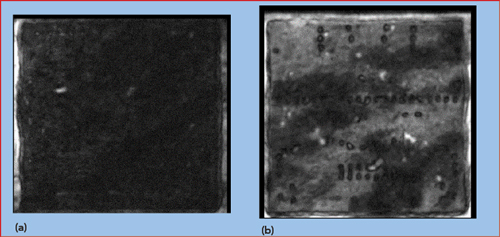
Figure 2 C-SAM images showing GaN die attach with largely void-free solder coverage (a) and excessive voiding (b).
The thermal conductivity of the baseplate material holding the die must also be maximized. For lower power applications, die is often installed on a Kovar™ baseplate, chosen because of its matched coefficient of thermal expansion (CTE). However, when thermal conduction is critical, a material such as copper molybdenum (CuMo) is a better choice. The process of choosing materials to optimize the thermal conductivity of each interface continues through the entire design, from device to system packaging.
While this thermal design approach is used for GaN amplifier designs regardless of application, it is particularly important for space-qualified hardware. The size and weight constraints common to space programs increase power density by limiting the volume, while the reliability requirements for space operation require maximum cooling of the active devices.
GaN RELIABILITY
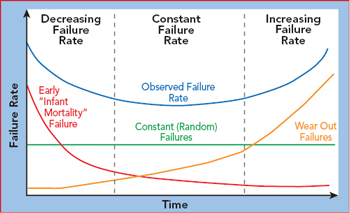
Figure 3 Reliability bathtub curve. Source: Wikimedia.
Reliability is often characterized by the failure rate versus time, which often looks like a “bathtub” and has been called the “bathtub curve” (see Figure 3). Typically, the majority of failures occur early in the product’s life or after considerable use. Early failures are usually caused by a manufacturing defect, either during device fabrication or subsequent assembly. On the other side of the graph, the uptick in failures represents the device wearing out near the end of its lifetime. To optimize and assure reliability, each of these failure types must be considered.
In the case of GaN, early failures are reduced through manufacturing process control, wafer screening and burn-in. Process control includes repeatable die attach, discussed above, and control of all aspects of the manufacturing process. Clear documentation and operator training are critical, as well as environmental controls, such as reducing the risk for damage caused by electrostatic discharge (ESD). With minimal performance variation across a GaN wafer, sample testing can be used to qualify a wafer, improving confidence in the device’s reliability before committing the devices from a wafer to assembly. Depending on the program, wafer screening may require accelerated life testing and destructive physical analysis. The risk of early failure can be reduced further through 100 percent burn-in screening. Using burn-in, amplifiers are biased and placed in an oven at elevated temperature for a specified time to stress the active devices. Burn-in screening will weed out the early failures, reducing the probability of failure in the field.
To quantify the length of operational time before wear-out failures occur, the MTBF of the amplifier is calculated. This calculation uses multiple factors such as device temperature, bias and environmental conditions and is based on empirical data from accelerated life testing. To maximize the MTBF, the device cooling must be optimized, as described earlier.
While the radiation encountered in space creates another reliability risk, the high molecular bond strength of GaN results in a higher radiation tolerance than GaAs and silicon.
CUSTOM GaN AMPLIFIER DESIGN
Since space missions usually require amplifiers with unique frequencies, bandwidths, output power and reliability, they usually require custom designs rather than off-the-shelf products. Since the production volumes are typically low, the cost of the development must be minimized as well as the unit cost, to keep the total program cost low. One of the best ways to reduce design time and cost is to improve first-pass success, which requires accurate device modeling.
Nonlinear device modeling for power amplifier design is always a challenge; since GaN is a newer technology, its models are less mature. To address this lack of accurate models, the design engineer has several options:
- Rely on measured load-pull data to determine the ideal output impedance match to optimize the RF power.
- Through experience, adjust the simulation models to improve the accuracy for the specific design conditions.
- Substitute a measured, small-signal S-parameter file for the nonlinear model to confirm similar results for linear operation.
SUMMARY
Satellite applications will clearly benefit from space-qualified GaN power amplifiers, which offer size, weight and thermal benefits over TWT amplifiers. However, producing GaN power amplifiers is challenging, particularly with the lack of space heritage. Successful insertion requires experience with both the electrical and mechanical aspects of GaN amplifier design, complementing space quality levels and requirements such as MIL-PRF-38534 class K. For organizations with both competencies, space-qualified GaN technology offers exciting new market opportunities.