
Figure 6 shows a micrograph with a chip area of 0.514 mm × 0.622 mm, including all test pads. The circuit is measured on wafer. An HP4142B voltage and current source is used to supply the DC voltages and the output is connected through a ground-signal-ground probe to the Keysight N9030A spectrum analyzer with a phase noise measurement utility and a 50 Ω load. The VCO is biased with VDD = 5 V and IDD = 6.2 mA. It consumes 31 mW of DC power.
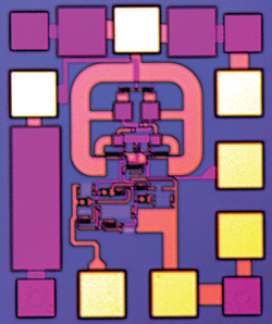
Figure 6 VCO IC.
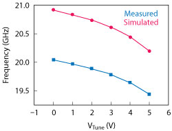
Figure 7 Simulated and measured VCO frequency vs. tuning voltage.
The oscillation frequency variation as a function of control voltage is plotted in Figure 7. When the control voltage is tuned from 0 to 5 V, the VCO operates from 20.04 to 19.44 GHz. That is, the VCO exhibits a tuning range of 3.04 percent based on a 19.74 GHz center frequency. The measured oscillation frequency (20.04 to 19.44 GHz) of the VCO is shifted down slightly as compared to the simulated oscillation frequency (20.92 to 20.2 GHz). The difference between the simulated and measured results can be attributed to the fact that all the passive elements and wiring of circuit were modeled with the quasi 3D electromagnetic simulation of momentum electromagnetic (EM) simulator in ADS. It is difficult to set the substrate parameters to be the same as those fabricated from the list in the library. Figure 8 shows the measured signal output power, which is above -10 dBm over the output frequency range.
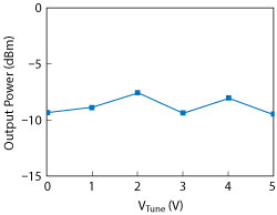
Figure 8 Measured VCO output power vs. tuning voltage.
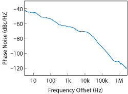
Figure 9 Measured VCO phase noise.
Phase noise of the VCO is difficult to measure, due to spectrum jitter caused by noise from supply and tuning voltages. In this work, the phase noise is roughly measured using the Keysight N9030A phase noise utility. Figure 9 shows the measured results. VCO phase noise is -111.8 dBc/Hz at 1 MHz offset from the 19.78 GHz carrier frequency.
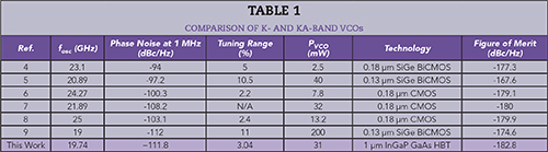
Table 1 compares this performance with that of previously reported VCOs in K- and Ka-Band. The commonly used figure of merit (FOM), which accounts for phase noise (PN), oscillation frequency (fosc), frequency offset (△f) from fosc, and power dissipation (PVCO) as depicted in Equation 3,6 is used for the comparison.
It is evident from Table 1 that, the VCO reported in this work has an excellent FOM compared with the other oscillators processed in SiGe BiCMOS or CMOS technology. Furthermore, its power consumption is remarkably low, only 31 mW, compared with other VCOs realized in the same InGaP GaAs HBT technology.17-18
CONCLUSION
A K-Band VCO in InGaP GaAs HBT technology operates at a high oscillation frequency with low phase noise. It employs a push-push negative gm architecture, which takes its output signal from a capacitive base CN of the cross-coupled transistors. Measurements demonstrate an oscillation frequency range from 19.44 to 20.04 GHz. Phase noise is -111.8 dBc/Hz at 1 MHz
offset from 19.78 GHz carrier.
ACKNOWLEDGMENT
This project is supported by the National Basic Research Program of China (Grant No. 2010CB327505), the Advance Research project of China (Grant No. 51308xxxx06), the Advance Research Foundation of China (Grant No. 9140A08xxxx11DZ111), the Doctoral Scientific Research Foundation of Henan University of Science and Technology (Grant No. 400613480011) and the Foundation of He’nan Educational Committee (Grant No. 15A510001).
References
- J. Zhang, Y. Zhang, H. Lu, Y. Zhang and L. Min, “A Novel Model for Implementation of Gamma Radiation Effects in GaAs HBTs,” IEEE Transactions on Microwave Theory and Techniques, Vol. 60, No. 12, December 2012, pp. 3693–3698.
- J. Zhang, Y. Zhang, H. Lu, Y. Zhang and Y. Shi, “The Model Parameter Extraction and Simulation for the Effects of Gamma Irradiation on the DC Characteristics of InGaP GaAs Single Heterojunction Bipolar Transistors,” Microelectronics Reliability, Vol. 52, No. 12, December 2012, pp. 2941–2947.
- X. Yu, A. El-Gouhary and N. M. Neihart, “A Transformer-Based Dual-Coupled Triple-Mode CMOS LC-VCO,” IEEE Transactions on Microwave Theory and Techniques, Vol. 62, No. 9, September 2014, pp. 2059–2070.
- H. Yinkun, W. Danyu, Z. Lei, J. Fan, W. Jin and J. Zhi, “A 23 GHz Low Power VCO in SiGe BiCMOS Technology,” Journal of Semiconductors, Vol. 34, No. 4, April 2013.
- J. He, J. Li, D. Hou, Y. Z. Xiong, D. L. Yan, M. A. Arasu and M. Je, “A 20 GHz VCO for PLL Synthesizer in 0.13 μm BiCMOS,” IEEE International Symposium on RF Integration Technology, November 2012, pp. 231–233.
- J. Yang, C. Y Kim, D. W. Kim and S. Hong, “Design of a 24 GHz CMOS VCO With an Asymmetric-Width Transformer,” IEEE Transactions on Circuits and Systems—II: Express Briefs, Vol. 57, No. 3, March 2010, pp. 173–177.
- S. Wang and W. J. Lin, “A K-Band Gm Boosting Differential Colpitts VCO in 0.18 μm CMOS,” Asia-Pacific Microwave Conference Proceedings, November 2013, pp. 1042–1045.
- T. Y. Lian, K. H. Chien and H. K Chiou, “An Improved Gm-Boosted Technique for a K-Band Cascode Colpitts CMOS VCO,” Asia-Pacific Microwave Conference Proceedings, November 2013, pp. 685–687.
- W. Wang, Y. Takeda, Y. S. Yeh and B. Floyd, “A 20 GHz VCO and Frequency Doubler for W-Band FMCW Radar Applications,” IEEE 14th Topical Meeting on Silicon Monolithic Integrated Circuits in RF Systems, January 2014, pp. 104–106.
- S. Kang, J. C. Chien and A. M. Niknejad, “A W-Band Low-Noise PLL With a Fundamental VCO in SiGe for Millimeter-Wave Applications,” IEEE Transactions on Microwave Theory and Techniques, Vol. 62, No. 10, October 2014, pp. 2390–2404.
- P. Andreani, X. Wang, L. Vandi and A. Fard, ”A Study of Phase Noise in Colpitts and LC-Tank CMOS Oscillators,” IEEE Journal of Solid-State Circuits, Vol. 40, No. 5, May 2005, pp. 1107–1118.
- P. Su, S. Zhao and Z. Tang, “Ku-Band Push-Push VCO Based on Substrate Integrated Waveguide Resonator,” Microwave Journal, Vol. 56, No. 5, May 2013, p. 166.
- H. Shin and J. Kim, “A 17 GHz Push-Push VCO Based on Output Extraction From a Capacitive Common Node in GaInP/GaAs HBT Technology,” IEEE Transactions on Microwave Theory and Techniques, Vol. 54, No. 11, November 2006, pp. 3857–3863.
- T. Nakamura, T. Masuda, K. Washio K and H. Kondoh, “A Push-Push VCO With 13.9 GHz Wide Tuning Range Using Loop-Ground Transmission Line for Full-Band 60 GHz Transceiver,” IEEE Journal of Solid-State Circuits, Vol. 47, No. 6, June 2012, pp. 1267–1277.
- M. Stuenkel and M. Feng, “A W-Band Tunable Push-Push Oscillator With 128X Frequency Division for Frequency Synthesis Applications,” IEEE MTT-S International Microwave Symposium Digest, June 2012, pp. 1–3.
- M. A. Margarit, J. L. Tham, R. G. Meyer and M. J. Deen, “A Low-Noise, Low-Power VCO With Automatic Amplitude Control for Wireless Applications,” IEEE Journal of Solid-State Circuits, Vol. 34, No. 6, June 1999, pp. 761–771.
- Y. Ting, Y. Zhang, H. Lu, Y. Zhang, W. Yue and L. Yifeng, “Low Phase Noise GaAs HBT VCO in Ka-Band, Journal of Semiconductors, Vol. 32, No. 2, February 2015.
- J. Zhang, Y. Zhang, H. Lu, Y. Zhang, L. Bo, L. Zhang and X. Fei, “A Ku-Band Wide-Tuning-Range High-Output-Power VCO in InGaP GaAs HBT Technology,” Journal of Semiconductors, Vol. 36, No. 6, June 2015.
Jincan Zhang received his M.S. degree and Ph.D. degrees from Xi’an University of Technology in 2010 and 2014, respectively. He is currently a lecturer at Henan University of Science and Technology. His research is focused on modeling of HBTs and the design of very high speed integrated circuits.
Hongliang Lu received her M.S. and Ph.D. degrees in microelectronics engineering from Xidian University in 2003 and 2007, respectively. Since 2010, she has been a professor in the School of Microelectronics at Xidian University. Her work involves modeling and experiments on SiC MESFETs and other devices.
Yuming Zhang received his M.S. and Ph.D. degrees in microelectronics engineering from Xidian University and Xi’an Jiaotong University in 1992 and 1998, respectively. From 1999 to 2000, he was with Rutgers University as a postdoctoral fellow. Since 2001, he has been a professor at the Microelectronics Institute, Xidian University. His research is in the design, modeling, fabrication and electrical characterization of SiC electronic devices for high temperature and high-power operation.
Yimen Zhang is a professor of the School of Microelectronics, Xidian University. He has been a visiting scholar and senior visiting scholar at Arizona State University, Tempe, and Yale University, respectively. His research interests are in the areas of wideband semiconductor devices, semiconductor devices modeling, TCAD for VLSI and quantum well devices.
Bo Liu received his B.E., M.S. and D.E. degrees in electronic engineering from the University of Kitakyushu, Japan in 2005, 2008 and 2012, respectively. Since 2012, he has been an associate professor at Henan University of Science and Technology. His research interests include VLSI layout design and process variation analysis for analog IC design for manufacturability.
Leiming Zhang received his M.S. degree at the University of Electronic Science and Technology of China in 2008. He is currently a lecturer at Henan University of Science and Technology. His research is focused on device modeling of CMOS and design of mixed signal integrated circuits.
Ligong Sun received his M.S. degree from Henan University of Science and Technology in 2006. He is currently an associate professor in Henan University. His research is focused on AI and robot, computer application technology and the design of mixed-signal integrated circuits.