

 MatchCalc
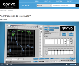
Qorvo MatchCalc is a free downloadable RF/microwave matching calculator with ideal tunable passive components. It displays the impedance of the input and output match in a 50 Ω test environment as measured on a network analyzer. Some of its key features are; displays insertion loss/gain of S1P and S2P files, real-time optimization and tuning, plot markers, snap-shot feature to hold static plots, on-tool transmission-line calculator, return loss plots to all input and output ports, ability to create a match report in word and thru-line function that displays input source impedance and output load.
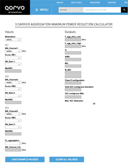 3 Carrier Aggregation Maximum Power Reduction Calculator
The maximum output power requirements for LTE user equipment is specified by the 3GPP TS 36.521 specifications and contains requirements for both the maximum output power as well as the output power tolerance. This calculator allows you to determine the maximum power reduction for three component carriers.
2 Carrier Aggregation Maximum Power Reduction Calculator
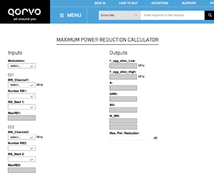 The maximum output power requirements for LTE user equipment is specified by the 3GPP TS 36.521 specifications and contains requirements for both the maximum output power as well as the output power tolerance. This calculator allows you to determine the maximum power reduction for two component carriers.
Trace Width Calculator
Calculating an accurate trace width is important in RF PC board design. Proper trace width is necessary to guarantee the desired DC current can be transported without overheating or damaging your PC board. 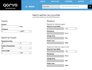 By providing input values such as current, board thickness, temperature rise, ambient temperature and trace length your able to calculate an estimate of the internal and external trace width layers for a given current and copper weight. The trace width design tool is based on the charts in IPC-2221 (A) equations.
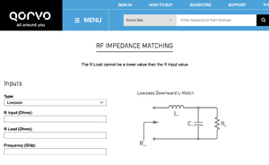 RF Impedance Matching Calculator
The L match circuit gets its name due to the circuit topology – resembling the letter “L”. This tool will help you create a matching circuit so optimal power transfer occurs between unmatched loads at a specific frequency. The calculator provides output data for circuit topology and component values.
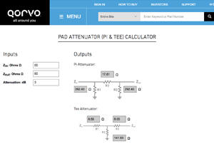 PAD Attenuator Calculator
This calculator is helps calculate the value of the resistors R1, R2 and R3 in a T-pad and Pi-pad attenuator. The user only needs to enter the attenuation in decibels (dB) and the given input and output characteristic impedance of the transmission lines to be matched.
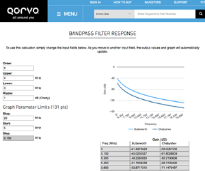 Bandpass Filter Response Calculator
This tool helps you analyze a Butterworth and Chebysheve filter response using frequency inputs. To use this calculator, you simply change the upper, lower frequencies as well as the order. For Chebyshev filter designs input the ripple in dB. As you move to another input field, the output values and graph will automatically update showing you the response of the filter.
Modelithics® Qorvo GaN Library
Qorvo and Modelithics collaborate to provide designers with high-accuracy nonlinear simulation models for  Qorvo GaN transistor devices. The Modelithics® Qorvo GaN Library has been developed using "best-in-class" measurement and modeling techniques. Modelithics is well-known for providing highly accurate measurement-based, advanced feature simulation models, offering powerful substrate and part-value scaling capability, instrumental in high frequency design. Modelithics' model libraries integrate seamlessly with the latest electronic design automation (EDA) simulation tools, and are thoroughly documented, with a model information data sheet for each model.
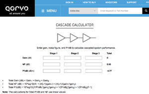 Cascade Calculator
RF Designers often require several parameter details when placing several amplifiers in a chain. This Qorvo Cascade Calculator provides performance values for system level gain, noise figure (NF) and P1dB for up to 3 cascaded power amplifiers in a chain. NF is the measure of an amplifier's contribution to the overall noise in the system. It is the ratio of the signal-to-noise ratio at the input of the amplifier to the signal-to-noise ratio at the output of the amplifier. P1dB or output power at 1 dB compression point, is the output power level at which the actual gain deviates from the small signal gain by 1 dB.
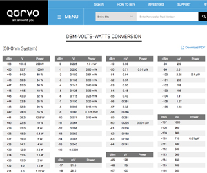 dBm Volts Watts Conversion
When designing RF power circuits, it’s useful to know the voltage level for a given power level. This table provides a chart showing the relationship between power in dBm, watts and the relevant voltage expressed in volts, millivolts and microvolts (peak-to-peak for sinusoidal signals) in a 50-ohm system. It is applicable for both low and high-power applications.
Noise Figure and Noise Temperature Calculator
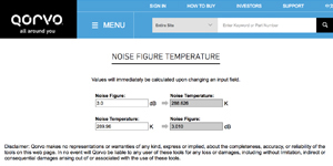 Noise figure and noise temperature are used interchangeably. NF measures degradation of the signal-to-noise ratio (SNR), which is caused due to RF and electronic components used in the transmit or receive chain. The noise figure number is displayed in decibels (dB), and represents the performance by which an amplifier or RF receiver can be measured. Noise temperature is the noise power of a component that is introduced into a system. The noise temperature is directly proportional to the temperature in degrees Kelvin.
PAE/Pdiss/Tj Calculator
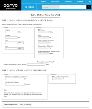 This calculator helps you calculate your power added efficiency (PAE), power dissipation and maximum junction temperature.
PAE is a measure rating the efficiency of a PA which considers the effect of the gain of the amplifier. PAE will be like efficiency when the gain of the amplifier is high.
Power dissipation is the process in which an electric device produces heat as an unwanted byproduct of its primary action. If a circuit current flows through a given element, losing voltage in the process, then the Pdiss by that circuit element is the product of the current and voltage (P = I x V).
Junction temperature is the highest operating temperature of the actual semiconductor in an electronic device.