
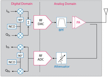
Figure 1 SDR example with digital predistortion feedback loop.
The design of radio frequency (RF) and microwave systems is usually based on the use of simplified representations of subsystems, often derived from datasheets, to predict overall system behavior. To reduce the number of design iterations, one needs a more accurate representation of “real” behavior. The common approach for RF design is to use measurement-based or electromagnetic (EM) simulated models, such as scattering parameters to represent the behavior of filters or linear amplifiers. These models capture the nonidealities more accurately. Unfortunately, when RF engineers use CAD/CAE tools for developing systems that include mixed-signal devices (where analog and digital waveforms coexist), they mainly use ideal approximations to represent the sampling circuit and the quantization subsystem or they assume them as being transparent to the RF signal, which degrades overall simulation accuracy.
Software-defined radio (SDR) front-ends are an example of mixed-signal system designs (see Figure 1) where components such as analog-to-digital converters (ADC) and digital-to-analog converters (DAC) are key elements of the overall design. The RF characteristics, specifically the input/output impedances of these components, may vary with frequency, such that a thorough characterization of the frequency response of the mixed-signal components will significantly improve the overall SDR design. For example, the ADC/DAC subsystems can be matched to the amplifier and filters of the RF transceiver. Figure 1 shows a transmitter with a feedback loop that implements real-time digital predistortion (DPD) to correct for distortion in the transmitter. To guarantee a properly corrected transmitted signal, the feedback loop itself should introduce no distortion. Due to the need for more signal bandwidth, recent SDR solutions require sampling rates to provide more than 1 or 2 GHz of DPD bandwidth. To limit the complexity and the cost of corrective circuits, an alternative to increased sampling rates is using higher Nyquist zones. However, this approach requires proper correction due to increased distortion in the feedback loop. To optimize the overall system and push it to its limits, better characterization and modeling approaches are needed for mixed-signal devices.
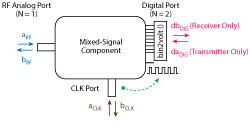
Figure 2 System-level representation of a mixed-signal component.
This article describes a key tool for RF engineers designing systems where analog and digital RF waveforms coexist. This work uses a new characterization approach and subsequent extraction of a mathematical model equivalent to scattering parameters for mixed-signal devices.1 This model is usable in system-level simulators to design 5G and other communication systems.
MIXED-SIGNAL SCATTERING PARAMETERS
In general, a mixed-signal system is considered, at least, as a three-port device, comprising the analog RF port, the digital bus and an additional port reflecting the sampling clock (local oscillator port). As it imposes a discrete time scale, the last port will determine and constrain the time sampling periods for the digital bus data. The focus of this approach is not on the individual bit-line operation,2 rather the information that the overall bitstream comprises. Therefore, the mixed-signal system will be characterized and modeled considering the entire digital bus as a single port (in other words, the digital port), which is sampled in time.
Figure 2 shows a representation of the system-level behavioral approach for mixed-signal systems. For consistency with their analog counterparts and to unify the formalism, incident and reflected digital signals are introduced conceptually. They are noted as dan and dbn voltage waves, respectively, where n represents the port number. The dan wave only exists in the transmit mode and the dbn wave only exists in the receive mode, where the other respective wave is considered zero. The sampled signal at the digital port is assigned to the proper voltage wave while being expressed in a 50 Ω characteristic impedance:
The generalization to the scattering waves formalism allows characterizing amplitude and phase over frequency for mixed-signal systems. This is similar to the well-known S-parameters for small-signal linear behavior and the polyharmonic distortion models,3 interconnected X-parameters4 or S-functions for large-signal operating points.5 This generalized formalism for mixed-signal components is referred to as D-parameters™.
To simplify the model formulation, the three-port mixed-signal system is reduced to a two-port mechanism by incorporating the clock (CLK) signal into the model. This is similar to a mixer representation,6 where the local oscillator (LO) imposes the point of operation. The D-parameter formulation for linear characteristics, as it will be employed throughout this article, is represented by:
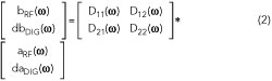
where ω represents the user-defined frequency grid, and daDIG and dbDIG are obtained for a specific state of the CLK signal (aCLK) and where the D-parameters are dependent on the LO drive.
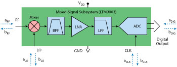
Figure 3 System-level characterization approach applied to the LTM9003.7
D11(ω) is equivalent to S11(ω) for an analog component and represents the matching performance of the RF port. Another measure is D21(ω), which is similar to the S21(ω) of a two-port analog network. It represents the frequency-dependent gain from the analog RF input port to the digital output port in a mixed-signal receiver. The amplitude and phase will depend on the LO drive. More specifically, the following parameters can be devised:
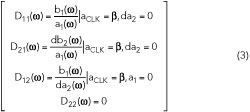

Figure 4 Mixed-signal measurement system.
Further details on the complete linear and nonlinear D-parameter formulation may be found in the original work.1
To present this approach more practically, a mixed-signal component is used to illustrate. The Linear Technology® LTM9003 wideband receiver7 (see Figure 3) is an RF-to-digital receiver subsystem that includes a 12-bit ADC, a bandpass filter (BPF), an intermediate frequency (IF) amplifier and a high linearity RF down-converting mixer.
MIXED-SIGNAL INSTRUMENTATION
For the simplest mixed-signal devices such as ADCs and DACs, the mixed-signal characterization test benches and mathematical formulations have been standardized by the IEEE for several years.8 This standard focuses on figures of merit, calculated for either the analog or digital side. It includes almost no information on characterizing and modeling the overall behavior.
To characterize and model mixed-signal components, the instrumentation industry has used a combination of instruments. Some of the capabilities have been integrated, leading to alternative solutions such as mixed-signal oscilloscopes. They accommodate analog and digital signals in a single instrument. However, these solutions have their limitations9 and were never capable of providing reliable RF-based characterization and modeling that enable the models to be used in the common RF/microwave simulators. During the last few years there have been several attempts to assemble a measurement test bench for specific mixed-signal cases.10-12 More recently, a different framework for the characterization and modeling of mixed-signal systems was developed, one that includes an idealized mixed-signal instrument architecture and the D-parameters formulation.
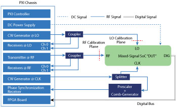
Figure 5 Architecture of the mixed-signal measurement system realized with the NI PXI platform.
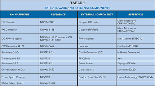
To deal with the characterization and modeling challenge of real- world applications, test and measurement systems need to follow the evolution of the devices under test, making a switch from traditional instruments—commonly divided by the type of signal to be measured—to a software-defined architecture that integrates all relevant hardware into a single measurement system. This article illustrates one such instrument based on modular PXI hardware and LabVIEW, which makes it possible to realize a flexible, stable and practical test bench for characterizing and modeling mixed-signal systems. The full mixed-signal system comprises several layers, from PXI hardware to LabVIEW software applications and some external components, shown in Figure 4. Two bidirectional couplers are employed at the RF and LO ports to allow measurement of the incident and reflected waves. This enables analog port calibration using a commercial short, open and load calibration kit. Additionally, a commercial power meter calibrates for absolute power, and an in-house developed comb generator (CG) is used to calibrate the absolute phase. This approach sets true calibration planes for the RF and LO ports (see Figure 5). To enable readers to duplicate the setup, Table 1 lists the instrumentation. To substitute for the “homemade” CG, any commercially available unit that accepts input frequencies from 1 to 250 MHz (the valid CLK range for the LTM9003) can be used.
MIXED-SIGNAL CHARACTERIZATION, MODELING AND SIMULATION
To demonstrate the capabilities and benefits of the measurement setup and the potential of mixed-signal scattering parameters, a practical example using the Linear Technology LTM9003 in the feedback loop of a DPD circuit is discussed. The goal of a DPD feedback loop is to generate a correction signal that eliminates the distortion generated by the power amplifier. The LTM9003 circuit sampling the output signal to generate the error information should not distort what is present at the output. Practically, however, the signal will be distorted, especially if one uses higher Nyquist zones to minimize the sample frequency and cost. Characterizing, modeling and compensating the feedback loop while linearizing is a solution to this problem. For this purpose, two LabVIEW applications were developed to obtain the RF performance and the RF-to-IF behavior of the LTM9003.
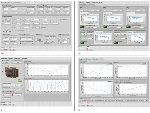
Figure 6 LabVIEW application frames: configuring the system (a), calibrating the measurement test bench (b), measuring the mixed-signal LTM9003 (c) and presenting the calibrated results (d).
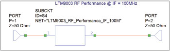
Figure 7 Mixed-signal LTM9003 D-parameters imported into the NI AWR Design Environment.
The first software application obtains the LTM9003 RF performance (D11(ω) and D21(ω)), extracting the performance across the complete range of RF frequencies with a fixed IF. This IF is already in the digital domain and can be selected by the user. From the internal architecture of the mixed-signal IC, the LO signal must follow the RF sweep in either the sum (LO = RF + IF) or difference mode (LO = RF − IF). After calibrating and performing the measurement sweeps, data processing will give D11(ω), which is required to understand the impact of RF input matching, and D21(ω), which is the frequency-dependent gain from the RF input to a fixed digital IF. Both amplitude and phase characteristics are obtained, relating the device signals in the analog and digital domains. This information is essential to allow small-signal simulation of the mixed-signal system with the other RF components using microwave simulators. The LabVIEW frames are shown in Figure 6, following the sequential steps to display the final calibrated measurements.
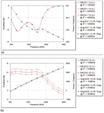
Figure 8 D-parameters, in amplitude and phase, obtained for the RF performance application, with D11 (a) and D21 (b) imported into the simulation tool at different IF frequencies.
The RF-to-IF LabVIEW application characterizes the digital IF frequency behavior and is obtained by sweeping the RF vs. frequency while keeping the LO frequency fixed, which forces the received IF signal to vary. The RF input matching should be close to or equal in frequency to the RF performance application for the full frequency range. A transfer function between the analog input at RF port (aRF) and the digital output (dbDIG) can be defined as the equivalent “gain” for the mixed-signal receiver, denoting the bandwidth performance of the device under test (DUT) and approximating, in this case, filter-like behavior. This measurement can be obtained for different clock (aCLK) values and LO (aLO) excitation frequencies and input power levels, resulting in a complete functional model. These models for mixed-signal components are important to simulate and optimize the overall performance. This LabVIEW application is similar in shape to the RF performance shown in Figure 6, so it is not included here.
The next step uses the previously extracted data in RF circuit and system simulators such as Microwave Office (circuit) and Visual System Simulator™ (system). As the acquired D-parameter files (*.d2p) are compatible with the SnP Touchstone format (*.s2p) used for S-parameters, these files can be loaded directly into these simulators to obtain relevant information (see Figure 7).
Figure 8 shows the D11 and D21 for the LTM9003, with a CLK frequency of 250 MHz. The curves observed in the D21 amplitude response show different gain values for the various IF frequencies measured. The D21 unwrapped phase component of the RF performance (shown in Figure 8b) represents the physical delay or group delay of the DUT between the analog and digital ports for the given CLK frequency. In comparison, Figure 9 shows the D21 phase component for the RF-to-IF performance normalized to 2π when using different frequency grids, which indicates a dependency between the CG grid and the CLK frequency. Also, it is easy to see the different Nyquist zones (multiples of CLK frequency) for the different grids. The D21 amplitude component depicts the expected BPF behavior. Figure 10 shows the LO port performance as a function of frequency.
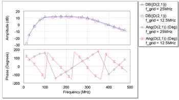
Figure 9 RF to IF behavior, in amplitude and phase, obtained for an LO of 1 GHz when RF is swept for different frequency grid steps.
The LabVIEW applications offer diverse possibilities to further integrate this data into more complex configurations. With this new approach it is now possible to integrate mixed-signal analysis into the NI AWR Design Environment and optimize subsequent analog components inserted in the system, such as filters, matching networks and amplifiers.
Conclusion
This article addressed the D-parameter framework, practical implementation of a PXI-based characterization system for D-parameter extraction and examples of integrating the information into RF/microwave simulators. This approach provides a complete framework for characterizing mixed-signal devices, whether systems on chip or full discrete systems. This type of characterization is important for SDR system designers and DPD-PA optimization. Characterizing mixed-signal components is an important step in the optimization of these circuits, particularly when considering impairments or limitations in the feedback loop chain.13-14
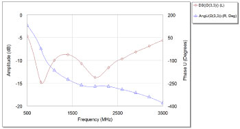
Figure 10 LTM9003 LO port wideband matching performance.
References
- D. C. Ribeiro, A. Prata, P. M. Cruz and N. B. Carvalho, “D-Parameters: A Novel Framework for Characterization and Behavioral Modeling of Mixed-Signal Systems,” IEEE Transactions on Microwave Theory and Techniques, Vol. 63, No. 10, October 2015, pp. 3277-3287.
- A. Ferrero, V. Teppati, E. Fledell, B. Grossman and T. Ruttan, “Microwave Multiport Measurements for the Digital World,” IEEE Microwave Magazine, Vol. 12, No. 1, February 2011, pp. 61–73.
- D. Root, J. Verspecht, D. Sharrit, J. Wood and A. Cognata, “Broadband Poly-Harmonic Distortion (PHD) Behavioral Models From Fast Automated Simulations and Large-Signal Vectorial Network Measurements,” IEEE Trans. Microw. Theory Techn., Vol. 53, No. 11, November 2005, pp. 3656–3664.
- D. E. Root, J. Verspecht, J. Horn and M. Marcu, “X-Parameters,” Cambridge, U.K., Cambridge Univ. Press, 2013.
- M. Myslinski, F. Verbeyst, M. Vanden Bossche and D. Schreurs, “S-functions Behavioral Model Order Reduction Based on Narrowband Modulated Large-Signal Network Analyzer Measurements,” 75th ARFTG Microwave Measurement Conference, Anaheim, CA, 2010, pp. 1–6.
- D. Williams, F. Ndagijimana, K. Remley, J. Dunsmore and S. Hubert, “Scattering-Parameter Models and Representations for Microwave Mixers,” IEEE Trans. Microw. Theory Techn., Vol. 53, No. 1, January 2005, pp. 314–321.
- Linear Technology®, LTM9003 Datasheet, “12-bit Digital Pre-distortion μModule Receiver Subsystem,” www.linear.com/product/LTM9003-AA.
- IEEE Standard for Terminology and Test Methods for Analog-to-Digital Converters, IEEE Standard 1241-2010 (revision of IEEE Standard 1241-2000), January 2011.
- P. Cruz, N. Carvalho and K. Remley, “Designing and Testing Software-Defined Radios,” IEEE Microwave Magazine, Vol. 11, No. 4, June 2010, pp. 83–94.
- P. Cruz, N. Carvalho, K. Remley and K. Gard, “Mixed Analog-Digital Instrumentation for Software-Defined-Radio Characterization,” IEEE MTT-S IMS Digest, June 2008, pp. 253–256.
- D. C. Ribeiro, P. M. Cruz, A. Prata and N. B. Carvalho, “Automatic Characterization of RF DACs for Software Defined Radio Applications,” IEEE MTT-S IMS Digest, June 2014, pp. 1–4.
- D. Ribeiro, P. Cruz and N. B Carvalho, “Synchronous Over-sampled Measurements for the Extraction of Mixed-Signal Behavioral Models in Digital to Analog Integrated Transmitters,” IEEE Trans. Microw. Theory Techn., Vol. 62, No. 12, December 2014, pp. 3183–3192.
- A. Prata, D. C. Ribeiro, P. M. Cruz, A. S. R. Oliveira and N. B. Carvalho, “Improving DPD Performance By Compensating Feedback Loop Impairments in RF ADCs,” IEEE MTT-S International Microwave Symposium, Phoenix, AZ, 2015, pp. 1–4.
- A. Prata, D. C. Ribeiro, P. M. Cruz, A. S. R. Oliveira and N. B. Carvalho, “RF Subsampling Feedback Loop Technique for Concurrent Dual-Band PA Linearization,” IEEE Transactions on Microwave Theory and Techniques, Vol. 64, No. 12, December 2016, pp. 4174–4182.