

The GaN market seems poised to take off this year as it becomes mainstream and starts penetrating some of the higher volume commercial markets. It has taken a strong foothold in most high power military applications and captured some of the cable TV and cellular infrastructure markets, but LDMOS still has the largest market share in the infrastructure and industrial markets. That might change soon, as GaN has as good or better performance than LDMOS and is now addressing the cost issue that seems to be the only advantage favoring LDMOS in most applications. Recent announcements by Qorvo, to move to 6 inch GaN on SiC, and MACOM, to prove 8 inch GaN on Si processed on low cost CMOS lines, will greatly reduce the cost of GaN, probablymaking it competitive with LDMOS. GaN also competes with GaAs in many of the higher frequency power markets and has displaced it in most of the future military applications where power is the most important performance specification.
If you do not have access to RF GaN device manufacturing within your company, you need to find a reliable GaN foundry service. While there are many RF GaN wafer fabrication facilities around the world, many of them are captive and not available to design companies that need their products manufactured. There does not seem to be much information generally available about RF GaN foundry services, so Microwave Journal surveyed as many of the GaN foundry services as we could identify and have summarized our findings.
General Landscape
There are several GaN foundries in North America (including one in Canada), a couple in Europe, and Taiwan’s WIN Semiconductors is the largest non-captive compound semiconductor foundry. Although the Japanese have a large market share in RF GaN, we did not find any Japanese companies offering foundry services, including Sumitomo, one of the largest GaN producers. China has been buying and launching semiconductor companies at a fast rate to build a presence in both the analog and digital markets. Chengdu HiWafer Semiconductor Co. and Xiamen San’an Integrated Circuit Co. offer compound semiconductor foundry services, and both state they have 6 inch GaN processes released or under development. We were not able to obtain detailed information about their capabilities in time for this article.
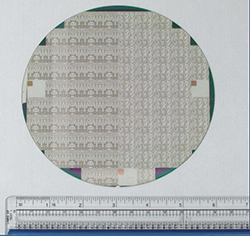
Figure 1 6 inch GaN on SiC wafer (courtesy BAE Systems).
In the U.S., a majority of customers use Wolfspeed (a Cree Company), while many European companies, especially in the aerospace and defense market, use United Monolithic Semiconductors (UMS) or OMMIC. Several companies have strategic relationships with specific foundries, with proprietary processes that are not available to other companies. An example is GCS, based in Torrance, Calif., who declined to provide process information for this survey, since their engagements are typically ITAR controlled or proprietary; they do partner with some companies to provide RF GaN foundry services. There are several captive RF GaN foundries, such as Raytheon, MACOM and Qorvo. As separate companies, RFMD and TriQuint offered GaN foundry services; since merging to become Qorvo, they only work with “strategic” customers, from the feedback we received.
Substrates
Most RF GaN devices are produced on SiC substrates, which offer a good lattice match and provide the high thermal conductivity that GaN demands—since its power density is very high compared to other semiconductor materials. Getting the heat out of the device is a huge challenge, so substrate and package materials are both critical. One company bucking that trend is MACOM, as they have the IP rights to International Rectifier’s original patents for GaN on Si (which MACOM acquired with Nitronex). Si substrates are much lower in cost than SiC but have lower thermal conductivity than SiC. The lower thermal conductivity arguably puts Si at a disadvantage compared to SiC. However, MACOM has published data showing with appropriate design, GaN on Si performs as reliably as GaN on SiC in many applications.1 GaN on Si could have the advantage of being processed on larger wafers on standard, low cost CMOS production lines. MACOM, however, does not offer foundry services; while they partner with GCS to produce GaN on Si devices, it is a proprietary process not available to other companies. We did find that OMMIC offers a GaN on Si process as a foundry service. OMMIC is the only company other than MACOM that we found offering RF GaN on Si devices.
All of the foundries surveyed process on 3 or 4 inch GaN wafers, but many plan to migrate to 6 inch as demand increases. Several have already announced plans to convert to 6 inch within the next year or two. BAE Systems estimates that converting from 4 to 6 inch GaN wafers (see Figure 1) will reduce the cost from ~$3/mm2 to ~$1.50/mm2, as the usable area about doubles.
Foundry Process Overview
In general, most foundries offer two or three standard processes: a 0.5 µm, high voltage (40 to 50 V) process aimed at high power devices for frequencies below approximately 8 GHz and a 0.25 µm, medium voltage (28 to 30 V) process for higher frequency applications (up to approximately 18 GHz). Some offer a third option, an even smaller gate length (typically, about 0.15 µm) for millimeter wave applications (up to 100 GHz). See Table 1 for a full listing of the processes offered by the seven companies that responded to our RF GaN foundry services survey.
Maximum power densities ranged from 6 to 8 W/mm, with Wolfspeed reporting a high of 8 W/mm for their 50 V, 0.4 µm G50V3 process. Other high power density processes of 6 W/mm or greater are available from BAE Systems, Fraunhofer, National Research Council of Canada, WIN Semiconductors and Wolfspeed. The highest operating frequency processes were Fraunhofer’s GaN10, with 0.1 µm devices operating to 94 GHz, and OMMIC’s D006GH (in development), with a 60 nm device operating to 100 GHz. Several foundries have efficiency exceeding 60 percent, including BAE, Fraunhofer, Wolfspeed, UMS and WIN. Most of the processes have field plates or offer them as an option. All of the foundries surveyed are using either 3 or 4 inch wafers, and a couple plan to move to 6 inch wafers relatively soon.
BAE Systems (Nashua, N.H.)
BAE Systems acquired the Lockheed Martin Sanders facilities in 2000. Their GaN processes are based on SiC substrates for best thermal properties, since they are geared to high performance military applications (with selected dual-use commercial markets when their process and/or design expertise are a good fit). This approach for military applications was first baselined by DARPA in 2005 under the Wide Bandgap Semiconductor-RF Program. Current wafer size is 4 inch. In 2014, they demonstrated high yield processing of MMIC power amplifiers (PA) on 6 inch wafers, using their field plate (FP) GaN process2 and are planning production release of a “no field plate” (NFP) process on 6 inch wafers in 2017.
BAE’s 0.2 µm field plate process, originally developed in the 2005 to 2008 timeframe, is now an industry standard process, with performance that is widely available in the market. Their newer NFP process offers high performance at an affordable cost. This includes high power, gain and efficiency up to 50 GHz. Using 2 mil thick wafers, small vias can be placed under every source for low inductance grounding. This, combined with reduced output capacitance (Cds) devices, enables wideband amplifiers with enhanced gain and power-added efficiency (PAE).3 The 140 V typical BVgd of the NFP process provides a high degree of robustness to high instantaneous voltages in PA designs, as well as high Pin survivability for low noise amplifiers (LNA). The 6 inch NFP GaN process will offer lower cost and leverage BAE Systems’ experience running 6 inch PHEMT processes for more than 10 years.4
Fraunhofer IAF (Freiburg, Germany)
Fraunhofer offers high performance processes with high efficiency. The company manufactures products for research, base stations, electronic warfare, point-to-point radio links and radar. Based on 4 inch GaN on SiC wafers, Fraunhofer offers three processes providing DC to 100 GHz coverage: 1) 0.5 µm gate length, 50 V operating voltage and a frequency range up to 6 GHz; 2) 0.25 µm, 28 V, to 20 GHz and 3) 0.1 µm, 15 V, to 94 GHz. The 0.5 µm process provides an efficiency of 65 percent with a power density of 6 W/mm. The 0.5 and 0.25 µm processes are fabricated on 4 mil thick wafers with 50 µm vias, while the 0.1 µm process is on 3 mil thick wafers with 30 µm vias. Fraunhofer allows foundry access every 4 months using pizza masks, with nearly arbitrary chip sizes in small quantities. Overall, they have good breath of frequency coverage with three gates lengths and provide high efficiency.
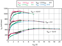
Figure 2 Pulsed I-V measurement on 2 × 20 µm cell, showing less than 10 percent gate lag on OMMIC’s D01GH GaN on Si process.
National Research Council of Canada (Ottawa, Canada)
We were surprised that the Canadian government, through the National Research Council (NRC), offers a full line of GaN foundry processes and is the only Canadian source for GaN electronics. Intended to aid Canadian industry and technology — but not restricted to working only within Canada’s borders — NRC serves both academic and commercial markets, leveraging its significant processing know-how. They offer one 0.5 µm and two 0.15 µm processes, operating up to 35 GHz, including probably the only enhancement mode process available on the market. The 0.15 µm depletion mode process has a power density of 7 W/mm, and the 0.5 µm process has a high breakdown of 180 V.
OMMIC (Limeil-Brévannes, France)
OMMIC offers foundry services and custom designs using its D01GH GaN on Si process that offers cost advantages over GaN on SiC. The process has a 0.1 µm gate length and runs on 3 inch wafers, planned to move to 6 inch in 2017. While this process was developed for power applications and provides 3.3 W/mm power density, it is also good for LNAs from 15 to 50 GHz, achieving a 1 dB noise figure at 30 GHz. Due to their ohmic contact regrowth process, D01GH devices exhibit very low noise performance, equivalent to state-of-the-art GaAs processes. In-situ passivation limits gate lag effects to less than 10 percent (see Figure 2), enabling better performance in switched mode applications such as radar. Their lower bias, 30 V breakdown devices, can be biased around 12 V VDD for PAs, with LNAs operating around 5 V. This is lower than other processes on the market, which mainly operate at 28 V.
OMMIC’s D006GH is a GaN on SiC process with 60 nm gate length. Still in development, the process will be released for foundry access in the first quarter of 2017. It is intended to support power and low noise applications from 40 to 100 GHz.
OMMIC’s development efforts are focused on PAs for Ka-Band satellite communications and X- and Ku-Band LNAs for military applications. In the next three years, they plan to focus on commercial markets, such as 5G base stations requiring Ka- and W-Band transmit/receive chips and instrumentation requiring DC to 67 GHz coverage and 32 dBm output power at 1 dB compression.
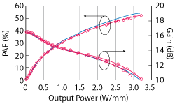
Figure 3 4 GHz PAE and gain vs. power density for 8 × 100 µm cell on UMS’ GH25 GaN on SiC process.
United Monolithic Semiconductors (Yvette, France)
Serving military, space and commercial (primarily telecom infrastructure and automotive) markets, UMS has developed and qualified two GaN on SiC processes. The 0.5 µm GH5010 process is suitable for power amplifiers operating up to C-Band and provides 5 W/mm with 50 V bias. The process is already listed in the European Space Agency (ESA) European Preferred Parts List (EPPL). The 0.25 µm GH25 MMIC process provides more than 4 W/mm with high efficiency up to Ku-Band (see Figure 3). Typical operating voltage is 30 V. This process also has good noise performance, typically 1.8 dB noise figure at 15 GHz with 11 dB associated gain. More than 60 GH25 foundry projects have already been launched.
To address higher frequency applications, to K- and Ka-Bands, UMS is developing a 0.15 µm process. UMS cites their EPPL listing as an indication that their process technology is high quality and reliable. They have a close link between their foundry technologies and UMS products, which ensures that the processes and models align with the needs of designers, are kept up to date and continuously improved. They offer express lots for short cycle time.
WIN Semiconductors (Tao Yuan City, Taiwan)
WIN Semiconductors, the largest compound semiconductor foundry, offers two GaN processes. As a pure-play foundry, WIN provides this technology via a non-competitive business model that insulates customers from potential conflict and supply chain risk. WIN’s GaN processes leverage their extensive GaAs production capabilities, and they support both discrete transistors as well as MMICs. They also offer a 28 V, high power, passive device process on 6 inch GaAs wafers and provide high Q passive networks for cost effective hybrid GaN products.
WIN’s primary commercial market for GaN technology is PAs used in wireless infrastructure. For military applications, their technology addresses PAs and LNAs used in radar systems. WIN presently offers two GaN HEMT technologies: NP25 and NP45. Both are fabricated on 4 inch SiC substrates. NP25 has a 0.25 µm gate with a source-coupled field plate and operates at 28 V. Typical power performance is 4 W/mm, with greater than 50 percent efficiency measured on a 1.25 mm cell at 6 GHz, biased at 28 V and 100 mA/mm. Linear gain is 17 dB. At 15 GHz, the process provides greater than 12 dB linear gain and 4.2 W/mm, with greater than 40 percent efficiency. The NP45 process has a 0.45 µm gate with a source-coupled field plate and operates at 50 V. Typical device performance is greater than 16 dB linear gain with greater than 6.5 W/mm and 60 percent efficiency, measured on a 4 mm cell tuned for peak output power at 2.7 GHz and biased at 50 V. The same device tuned for maximum efficiency (also at 2.7 GHz and 50 V bias) achieves over 75 percent efficiency, with approximately 5 W/mm and greater than 17 dB gain. This was the highest efficiency reported.
Wolfspeed (Durham, N.C.)
Wolfspeed, a Cree Company, is one of the most widely used foundries, offering four processes, all on 4 inch wafers. They cater to many military and commercial applications, such as wireless infrastructure, radar (both commercial and military), ISM, LMR, satellite communications, avionics, data links, space and CATV. They have 0.4 µm gate length processes with 50 and 28 V operating voltage, with the higher voltage process having a power density of 8 W/mm and a breakdown voltage exceeding 150 V. This was the highest reported power density we found for a GaN process. For higher frequency applications, Wolfspeed offers 0.25 µm processes that operate with 40 and 28 V bias that cover up to 18 GHz. All of their processes have efficiencies of 65 percent, which is very competitive among those reported.
Wolfspeed recently announced that their discrete transistors and multi-stage GaN MMICs have exceeded 100 billion total hours of field operation, the largest known body of field data accumulated by any domestic GaN supplier. Sumitomo is probably the only other RF GaN supplier that might have accumulated this history of field operation. Wolfspeed has achieved Category 1A trusted-foundry status through certification from the Defense MicroElectronics Activity (DMEA). Additionally, they have been assessed by the U.S. Department of Defense (DoD) as being at Manufacturing Readiness Level 8 or higher.
Reliability
Many of the military applications at BAE Systems impose challenging reliability requirements for their GaN MMICs. High baseplate temperatures and wideband CW operation result in high channel temperatures. All of their production GaN processes have been tested and qualified to ensure devices meet these demanding requirements. They perform accelerated life testing under RF drive at multiple temperatures, from which the activation energy is estimated and lifetime (MTTF) at actual operating temperatures calculated. The typical MTTF derived in this manner for BAE Systems’ 0.18 µm NFP GaN process is 107 hr at 200°C channel temperature, at its maximum recommended operating voltage of 30 V.
Fraunhofer performs DC, HTRB and RF testing at 2 and 10 GHz for their GaN50 and GaN25 processes. For the GaN10 process, they just test at 10 GHz.
NRC reports that reliability measurements for the GaN150 process are in progress. MTTF measurements on a previous process (GaN800) yielded an MTTF of 2.5 × 10⁷ hours at a channel temperature of 200°C.
OMMIC’s preliminary reliability tests show no significant degradation after 2000 hours of DC life testing with a case temperature of 80°C, Vds = 12 V and Ids = 200 mA/mm, which equates to a channel temperature of 200°C. Other reliability tests are underway.
UMS qualifies their processes by performing storage, HTRB, HTOL and DC life tests, as well as RF step stress and RF life testing. This enables them to determine maximum ratings and guarantee at least 20 years reliability at 200°C junction temperature. These qualification tests are performed on elementary cells, typical of those used in discrete devices and MMICs with larger gate widths.
For reliability verification, WIN provides customers with a full qualification report that includes four temperature MTTF results.
Wolfspeed’s processes have delivered more than 100 billion total hours of field operation with a FIT rate of less than 5 per billion device hours for discrete GaN RF transistors and multi-stage GaN MMICs. The company recently announced that their GaN RF power transistors completed testing and demonstrated compliance with NASA reliability standards for satellite and space systems. They partnered with KCB Solutions on a comprehensive testing program to demonstrate that their GaN on SiC devices meet NASA EEE-INST-002 Level 1 reliability and performance standards, derived from the MIL-STD requirements for Class S and Class K qualifications.
Backend Services
BAE Systems offers on-wafer test and wafer dicing, chip picking and inspection. First-level packaging is also offered to some customers. For example, they can deliver die soldered onto CTE-matched shims or assembled in simple packages.
All Fraunhofer SiC processes include full backside processing, including via holes with metallization upon request. They perform extensive testing (DC, small signal and load-pull wafer mapping) as well as full MMIC testing. They provide fast packaging of power bars for high-power characterization.
NRC offers on-wafer testing but no mounting or packaging.
OMMIC offers on-wafer test services, visual inspection (commercial and space grade), lot acceptance testing (LAT) and wafer acceptance testing (WAT) for space programs. Every design can be packaged in either plastic QFN (with up to 30 GHz operation) or air cavity packages. They also offer hermetic packaging services for space applications.
UMS offers a wide and flexible range of back-end services, including on-wafer noise and power testing. They also offer visual inspection, picking and packaging.
WIN provides high voltage DC product testing, dicing and inspection services for GaN customers.
Wolfspeed provides dicing, on-wafer DC/RF probe and fixtured DC/RF characterization.
EDA Software Support
BAE Systems offers design services on a case-by-case basis. They also provide design support to customers who wish to design their own MMICs. They have an internally-developed modified Angelov nonlinear model that is very accurate for nonlinear circuit simulation. They provide all necessary device models and layout information to foundry customers. ADS-compatible PDKs are under development and will be available in late 2016.
Fraunhofer has Keysight PDKs for microstrip and grounded coplanar transmission lines for ADS (ADS DRC included), including full auto-layout functions.
For the GaN500 process, NRC offers both Root and Angelov models in ADS. For GaN150, they only offer a Root model. No models are available for the 0.15 µm E-GaN process.
OMMIC PDKs are available on their website for the latest 32- and 64-bit versions of ADS and for the 32-bit version of NI/AWR Microwave Office. The 64-bit NI/AWR design kit is under development. For all design kits, they provide nonlinear models and noise models, all over temperature. They also provide a DRC and LVS checking service in house, if needed. They have a team of modeling engineers dedicated to customer support and offer a multi-project wafer (pizza mask) service with four runs a year per process, for small prototyping quantities.
UMS’ GH25 PDKs are compatible with ADS and Microwave Office. They include nonlinear, electro-thermal scalable models for power generation, linear models for LNA design, cold FET models for switches and diodes and passive elements for MMIC designs. Their PDKs include additional features such as DRC and 3D view generation for EM simulation.
WIN design kits are available for ADS and NI/AWR platforms and contain internally developed and optimized nonlinear models, models for small-signal and noise and load-pull data. WIN offers 24-hour design rule checking using a web-based tool, WebDRC. Layout verification (LVS) is done through Cadence as well as the ADS and AWR platforms.
Wolfspeed offers PDKs with ADS and NI/AWR’s Microwave Office.
Market Opportunities
Similar to the path taken by GaAs devices, expect GaN to mature and become the technology of choice for a diverse range of applications, especially the high power markets. As the technology proliferates and its cost declines, GaN will provide the best value for many PA functions where it offers an optimum trade-off. As communication and military systems become more complex, device specifications for transmit power, efficiency, linearity, frequency/bandwidth and operating temperature will become more challenging and GaN will offer many advantages over GaAs and Si. For example, in military applications, it improves size, weight and power (SWaP), and will continue to make inroads in those systems.
Most GaN suppliers see the base station and satellite markets as areas for major growth in the near term, with one foundry mentioning automotive. The millimeter wave portion of 5G could also be a large opportunity, as GaN performs well in broadband, high frequency applications. The RF Energy market is a good fit for GaN technology as well. Aerospace and defense markets that foundries see having the most growth include wideband, high power amplifiers for electronic warfare, phased arrays for radar and a wide range of millimeter wave applications.
GaN’s Future
The main competition for GaN is LDMOS at RF frequencies and GaAs for higher frequencies. LDMOS still dominates the high volume commercial markets for high power applications. While GaN will not completely replace any one technology, it is bound to further penetrate these higher volume markets as it becomes more price competitive. LDMOS continues to improve its performance each year, so it will remain competitive in these markets, yet it is bound to yield significant market share in the future.
BAE Systems thinks that in the long term, GaN for microwave applications will flourish in the applications where it is best suited: predominantly high power at frequencies from 1 to 100 GHz. Nonetheless, it won’t completely replace GaAs and Si, as these both have their own unique performance characteristics and associated economies that will ensure continued viability for certain markets. Further expansion of GaN will occur as high yield processes mature and wafer sizes increase, reducing costs. GaN clearly is a disruptive semiconductor technology, with no other semiconductor technology emerging to threaten it for at least the next decade.
Expect continued evolution of GaN variants such as GaN on Si for reduced cost and GaN on diamond for enhanced thermal properties for high performance applications. GaN will also be used more widely for functions other than PAs, such as LNAs, switches and multi-function MMICs. A combination LNA/limiter is well suited for GaN, with its combination of low noise performance and high breakdown voltage, the latter good for limiters.
The most interesting evolution will be the fight between GaN on SiC and GaN on Si. Will one technology win out in the industry? GaN on Si has the promise of being lower cost — offering larger wafer sizes and lower substrate and processing costs, if processed on standard CMOS production lines. If its performance is close to that of GaN on SiC, arguably, the cost advantage will be too great for SiC to overcome. On the other hand, SiC will have thermally-driven performance advantages that are required by some applications, ensuring a place for both technologies.
References
- Doug Carlson, “Commercialization of GaN,” Microwave Journal, June 2014, Vol. 57, No. 6, pp. 34–40.
- Isaak et al., “The First 0.2 µm 6-Inch GaN-on-SiC MMIC Process,” CS ManTech, 2014, pp. 229–231.
- Komiak et al., “Decade Bandwidth 2 to 20 GHz GaN HEMT Power Amplifier MMICs in DFP and No FP Technology,” IMS 2011.
- Gunther et al., The First 0.1 µm 6-Inch GaAs PHEMT MMIC Process,” CS ManTech, 2006, pp. 23–26.