
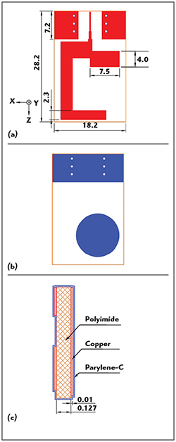
Figure 1 Monopole antenna geometry (dimensions in mm); top layer (a) bottom layer (b) cross section (c).
A small planar flexible monopole antenna with a parylene-c coating is designed for wireless local area network and the ultra-wideband system applications. It is fabricated on a polyimide film and consists of a folded and meandered radiating strip fed by a microstrip line. A parallel plate capacitor loads the open end of the radiating strip to reduce its size. The antenna operates from 2.4 to 2.484 GHz and from 3.8 to 10.6 GHz. Far field radiation patterns under bent conditions are also presented.
Flexible electronics are low profile, lightweight and have the capability to conform to curved surfaces.1 The previous decade has seen a great deal of research in flexible electronics for applications in areas such as health care, mobile communications, flexible displays, wearable individual communication devices and biomedical telemetry devices.2–3
Much effort has gone into the design of lightweight multiband antennas in order to combine communication standards such as wireless local area network (WLAN) and ultra-wideband (UWB) technology in a single portable device.4-6 WLAN covers frequency bands of 2.4 to 2.484 GHz, 5.15 to 5.35 GHz and 5.725 GHz to 5.825 GHz in accordance with the IEEE 802.11 WLAN standards. In 2002, the frequency band 3.1 to 10.6 GHz was officially allocated to unlicensed UWB communication applications by the Federal Communication Commission.
Monopole antennas have been extensively used in communication systems because they have uncomplicated structures and thin profiles, are lightweight and exhibit wideband characteristics. Diverse structures such as arc-shapes,7 half-elliptical-edges8 and u-shapes9 have been utilized. To further shrink antenna size and to improve input matching, several loading techniques including capacitive loading,10 inductive loading11 and multiresonator-loading9 have been proposed; however, most antennas incorporating loading techniques are not fabricated on a thin and flexible substrate.
This work describes a flexible capacitively-loaded monopole antenna that operates in both the WLAN and upper UWB frequency bands. The antenna, with a thickness of just 127µm, is coated with 10 µm of conformal parylene-c to for protection from corrosive agents. Input return loss, amplitude radiation patterns and gain under flat and flexed conditions show that the antenna may be bent or formed with minimal performance degradation. With the conformal parylene-c coating, it also has the capability to function normally in harsh environments.
ANTENNA CONFIGURATION AND DESIGN
The geometry and dimensions of the antenna are shown in Figure 1. Figure 2 is a photograph of the fabricated antenna (including a subminiature SMA connector), clearly demonstrating its flexibility. It is fabricated on a 127 µm thick Dupont Kapton HN polyimide film with a dielectric constant of 3.5 and a loss tangent of 0.0008. The overall dimensions are 28 mm × 18 mm.
The antenna has a double sided layout that includes a 50 Ω microstrip feed, a two stage impedance transformer, an open strip, a radiating meandered strip and a circular-plate loading capacitor. Two rectangular metal grounded strips on the top side are connected to the ground plane on the bottom side of the polyimide film with six metallized vias.
The two metal symmetrical grounded strips on the top side of the substrate are designed for the convenience of connecting an SMA end-launch connector for measurement. A two-stage impedance transformer is connected to the 50 Ω transmission line feed in order to improve wideband input impedance matching. A 7.5 mm length of open strip further optimizes the input return loss over the operating bands. The center frequency of the antenna is slightly tunable with strip length alteration.
The parallel-plate capacitor can be easily realized because the thickness of the polyimide substrate is only 127 µm. The circular patch on the bottom side of the substrate and the open end of the strip on the top side with a width of 2.3 mm together determine the loading capacitance. The capacitance of the loading capacitor with area S and the thickness d can be approximated by:
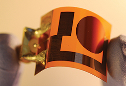
Figure 2 Photograph of the fabricated antenna.
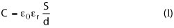
where εr is the permittivity (εr =3.5) of the polyimide substrate, ε0 is the electric constant (ε0 =8.85 × 10⁻¹²) and the area of the capacitor is about 3.01 × 10⁻⁶ m2. The calculated capacitance is about 0.7 pF.
Parylene-c is a commercially available product that is lightweight, unstressed, optically transparent and chemically/biologically inert. This makes it an excellent barrier material. Furthermore, it has a low dielectric constant (εr =2.95) and low loss (tanδ ≈ 0.002 at 6 GHz).12 In this design, parylene-c coating with the thickness of 10 µm is used to enhance reliability in harsh environments.
ANTENNA FABRICATION
Fabrication of the monopole antenna took place in the Wisconsin Center for Applied Microelectronics at the University of Wisconsin-Madison. The process is summarized in Figure 3. A 127 µm thick polyimide film (Dupont Kapton HN) is first cut using an ultraviolet laser for accurate via hole and rectangular device formation. The pre-cut film is laminated on top of a polydimethylsiloxane (PDMS) coated glass substrate, which is a conventional micro-fabrication process. A 1 µm thick copper layer is uniformly sputtered on the top side of the film and in the via holes, followed by photolithography-based copper etch-back process to form the circular patch and ground metal. The film is then flip transferred to another PDMS coated glass substrate for antenna patterning. With additional repetitive copper sputtering and etch-back, the antenna fabrication is complete. In the last stage, the fabricated antenna is de-laminated from the handling glass substrate.
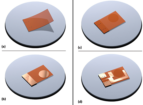
Figure 3 Fabrication process; laminate polyimide film on temporary substrate (a) deposit and etch back copper (b) delaminate and flip transfer onto different temporary substrate (c) deposit and etch back copper (d).
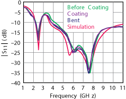
Figure 4 Simulated and measured antenna return loss.
An SMA end launch jack connector from Amphenol Connex is soldered to the microstrip feed line. Because the polyimide substrate is very thin, the soldering iron temperature is kept as low as possible (about 200º) during assembly to avoid melting.
The antenna with its SMA connector is then moved into the parylene coating chamber. A 10 µm conformal parylene-c coating is formed on the surface. First the solid parylene-c dimer is heated to about 150ºC in the vaporizer and undergoes pyrolysis. Then the gas parylene-c dimer is transformed into a monomer gas in a furnace. Finally, the monomers enter the vacuum deposition chamber at room temperature, becoming a thin film on the antenna polyimide substrate.
MEASURED RESULTS
Antenna input return loss, radiation patterns and gain are measured with a Satimo spherical near field measurement system. Figure 4 compares simulated and measured antenna return loss, showing good agreement. The fabricated antenna has a -10 dB impedance bandwidth in the frequency ranges of 2.4 to 2.484 GHz and 3.8 to 10.6 GHz. These correspond to WLAN and upper UWB communication frequencies bands, respectively.
Return loss with and without parylene-c coating is shown in Figure 4, as well, demonstrating that the 10 µm of parylene-c has no significant effect. This is because the dielectric constant of the parylene-c coating material is close that of the substrate material and is only 10 µm thick as compared to the substrate’s 127 µm thickness.
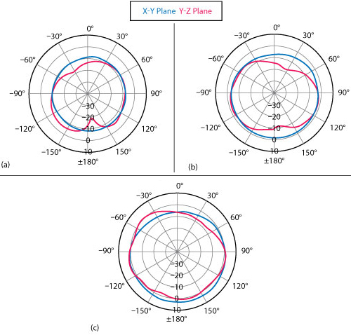
Figure 5 Measured radiation patterns at f = 2.44 GHz (a) f = 5.8 GHz (b) and f = 10.6 GHz (c).
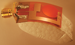
Figure 6 Antenna bent around a polystyrene foam mandrel.
The results shown in Figure 5 are the measured radiation patterns of the flat antenna in the anechoic chamber at 2.44 GHz, 5.8 GHz and 10.6 GHz. The peak gain of the antenna is about -3.8 dBi, 1.1 dBi and 2.8 dBi for 2.44 GHz, 5.2 GHz and 10.6 GHz, respectively.
Return loss of the antenna bent over polystyrene foam (εr = 1.06) with a radius of 40 mm, is shown in Figure 6. As seen in Figure 4, there is little difference between the return loss of the flat and bent antenna. Radiation patterns under the flat and bent conditions at 2.44 GHz and 5.8 GHz are compared in Figure 7. It is apparent that the antenna retains its omnidirectional radiation pattern despite being bent over the foam mandrel.
CONCLUSION
A flexible monopole antenna for WLAN and upper UWB applications is described. It is fabricated on a Dupont Kapton HN polyimide film and is coated with a parylene-c conformal coating that has excellent mechanical and electrical properties. The antenna is measured under bent conditions, exhibiting minimal degradation in return loss and radiation performance. Flexibility, simplicity of fabrication, good radiation characteristics and high reliability demonstrate the antenna’s suitability for use in flexible/conformable wireless applications
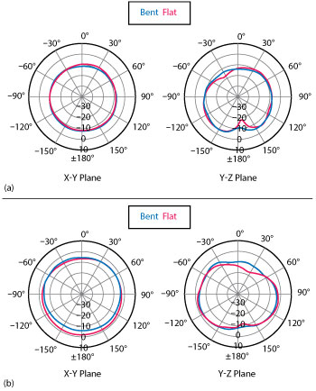
Figure 7 Antenna radiation patterns under flat and flexed (bent) conditions at f = 2.44 GHz (a) and f = 5.8 GHz (b).
Acknowledgments
This work was supported by a PECASE award under grant FA9550 – 09 – 1 – 0482 and National Natural Science Foundation of China (Grant No. 61474020). The program manager at AFOSR is Dr. Gernot Pomrenke. Yijie Qiu, Yei Hwan Jung and Subin Lee contributed equally to this article.
References
- A. Nathan, A. Ahnood, M.T. Cole, S. Lee, Y. Suzuki, P. Hiralal, F. Bonaccorso, T. Hasan, L. Garcia-Gancedo, A. Dyadyusha, S. Haque, P. Andrew, S. Hofmann, J. Moultrie, D. Chu, A. J. Flewitt, A. C. Ferrari, M. J. Kelly, J. Robertson, G. Amaratunga and W. I. Milne, “Flexible Electronics: The Next Ubiquitous Platform,” Proceedings of the IEEE, Vol. 100, May 2012, pp. 1486–1517.
- K. Zhang, J.H. Seo, W. Zhou and Z. Ma, “Fast Flexible Electronics Using Transferrable Silicon Nanomembranes,” Journal of Physics D: Applied Physics, Vol. 45, No. 14, March 2012, p. 143001.
- H.R. Khaleel, H.M. Al-Rizzo and D.G. Rucker, “Compact Polyimide-Based Antennas for Flexible Displays,” Journal of Display Technology, Vol. 8, No. 2, February 2012, pp. 91–97.
- K. Jun-Won, J. Tae-Hwan, R. Hong-Kyun, W. Jong-Myung, E. Chang-Soo and L. Dong-Kook, “Compact Multiband Microstrip Antenna Using Inverted-L- and T-Shaped Parasitic Elements,” IEEE Antennas and Wireless Propagation Letters, Vol. 12, September 2013, pp. 1299–1302.
- Q. Yijie, J. Yei Hwan, L. Subin, S. Ting-Yen, L. Juhwan, X. Yue Hang, R. Xu, W. Lin; N. Behdad and Z. Ma, “Compact Parylene-c-Coated Flexible Antenna for WLAN and Upper-band UWB Applications,” Electronics Letters, Vol. 50, No. 24, November 2014, pp. 1782–1784.
- A.T. Mobashsher and R.W. Aldhaheri, “CPW-Fed Folded Antenna With Forward-Directed Radiation Patterns for Handheld Dual-Band RFID Reader Applications,” Microwave Journal, Vol. 57, No. 2, February 2014, pp. 90–98.
- J. H. Lu and C. H. Yeh, “Planar Broadband Arc-Shaped Monopole Antenna for UWB System,” IEEE Transactions on Antennas and Propagation, Vol. 60, No. 7, July 2012, pp. 3091–3095.
- X. Kuiwen, Z. Zhongbo, L. Huan, H. Jiangtao, L. Changzhi and R. Lixin, “A Printed Single-Layer UWB Monopole Antenna With Extended Ground Plane Stubs,” IEEE Antennas and Wireless Propagation Letters, Vol. 12, February 2013, pp. 237–240.
- H. Wei, Y. Ying-Zeng, Y. Xi and F. Peng, “Compact Multiresonator-Loaded Planar Antenna for Multiband Operation,” IEEE Transactions on Antennas and Propagation, Vol. 61, No. 5, January 2013, pp. 2838–2841.
- L. Changrong, G. Yong-Xin and X. Shaoqiu, “Capacitively Loaded Circularly Polarized Implantable Patch Antenna for ISM Band Biomedical Applications,” IEEE Transactions on Antennas and Propagation, Vol. 62, No. 5, February 2014, pp. 2407–2417.
- M.A. Othman, T.M. Abuelfadl and A.M.E. Safwat, “Dual and Wide-Band Inductively-Loaded Dipole-Based Antennas for WLAN/UMTS Applications,” IEEE Transactions on Antennas and Propagation, Vol. 61, No. 3, November 2012, pp. 1430–1435.
- M. Jimin, B. Kim, D. Ha and W.J. Chappell, “Parylene Interposer as Thin Flexible 3-D Packaging Enabler for Wireless Applications,” IEEE Transactions on Microwave Theory and Techniques, Vol. 59, No. 12, December 2011, pp. 3410–3418