
A wideband high dynamic range low noise dual channel receiver front-end operates at 8.6 ± 0.4 GHz and has a 600 MHz intermediate frequency. It exhibits a maximum conversion gain of over 90 dB with 63 dB controllable. Over its entire 800 MHz bandwidth, gain fluctuation is less than 2.1 dB and noise figure is better than 1.8 dB. Its two channels are consistent with respect to gain, voltage standing wave ratio (VSWR) and noise figure. Its performance is suitable for high speed wireless communication or phased array applications.
Rapid growth in the communication technologies applied to third-generation networks is occurring throughout the world. CDMA2000 and other networks can currently provide data rates of several megabits per second (Mbps) or higher to individual users.1 According to the IMT-Advanced system definition, however, networks should support data rates up to 100 Mbps; so there is further work to be done.2-3 Yu et. al., describe a receiver operating at 6.1 GHz with 100 MHz bandwidth designed for a TDD system capable of supporting 1 Gbps wireless service,2 while Chen et. al., introduce a receiver designed to operate in Ku-Band with 100 MHz bandwidth for an FDD system.3 These are typical of high performance receivers for next generation multiple-input-multiple-output (MIMO) wireless communication.
In the pursuit of much higher data rates, the wireless communication standard Beyond 4G (B4G) is in deliberation. Massive MIMO is likely to be one of the key technologies in the B4G network. In order to deal with more devices and higher bit rates, massive MIMO uses hundreds of antennas at the base station that can serve many tens of terminals simultaneously. With a much greater scale, massive MIMO can reap all the benefits of conventional MIMO, while increasing capacity and significantly improving energy efficiency.4 High frequency, broad bandwidth, OFDM as well as MIMO technologies may all be employed in the B4G network.
One of the most important subsystems is the receiver front-end that amplifies the signal received by the antenna while suppressing interference and noise. Several hallmarks of a good receiver front-end include low noise figure, large dynamic range, high conversion gain and good image rejection.5 For systems consisting of multi-channel receivers such as massive MIMO or phased arrays, the emphasis is on channel size and weight reduction, power consumption, cost, reproducibility and reliability.6

X-Band has been exploited for use in many applications such as fire control radar, airborne systems, vehicle location systems and satellite communications.7-11 In this article, a dual-channel X-Band receiver front-end is designed for use in a massive MIMO system.
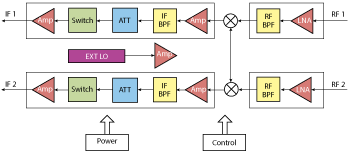
Figure 1 Simplified block diagram of the dual-channel RF receiver front-end.
Front-end Design
Architecture and Link Budget
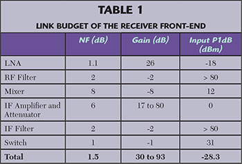
The receiver front-end consists of several major components, including low noise amplifiers, RF bandpass filters, mixers, IF amplifiers with digital attenuators, switches and IF filters. Figure 1 is a simplified block diagram. Using Keysight Advanced Design System (ADS) software, the link budget is simulated and optimized (see Table 1).
Low Noise Amplifier
The performance of the first amplifier is extremely important to ensuring a low receiver noise figure. In this X-Band two-stage design, a low noise Mitsubishi InGaAs HEMT (MGF4941) is used. Although this transistor is optimized at 12 GHz where Rn is at its lowest value, we chose it for its low cost and outstanding X-Band performance. Since the transistor itself is not unconditionally stable, a short-circuited microstrip line is placed at the source to improve stability. In addition, a quarter wavelength high resistance transmission line with a radial stub is used in the DC bias network as an RF choke.
Theoretically, to obtain low noise with high associated power gain, the first stage should use noise matching and the second stage should use complex conjugate matching. Considering the receiver front-end’s input return loss, however, a trade-off is made between optimal noise matching and gain matching for the first stage. Because the relative bandwidth of this LNA is not wide, all matching networks are L-type for simplicity.
Figure 2 Two-stage LNA PCB layout.
Simulation is done carefully because the transistor’s Rn at 8.6 GHz is larger than 5. This causes the S-parameters to be sensitive to errors in simulation and manufacturing. Mitsubishi’s nonlinear model is used. LNA S-parameters and noise figure are optimized through small signal analysis in ADS. Figure 2 shows the PCB layout of the two-stage LNA. Figure 3 summarizes the simulation results showing that the input and output VSWR is better than 1.2, the noise figure is less than 0.5 dB and the gain is larger than 27.2 dB. The LNA is unconditionally stable from 0 to 24 GHz.
Return loss performance is optimized by building the SMA connector model and microstrip line in HFSS, which shows that return loss can be increased with a tapered transition (see Figure 4a). W0 is chosen based on the characteristic impedance while Rc and Lc are the radius and length of the SMA connector’s inner conductor, respectively. According to the simulation, improvement is greater than 10 dB in comparison with an abrupt transition (see Figure 4b).
Figure 3 Two-stage LNA ADS simulation results: S-parameters (a) noise figure and stability factor (b).
RF Filter
Image rejection must be sufficient to mitigate the effects of jamming and interference.6 With the low noise amplifier preceding the image rejection filter, SSB noise figure is improved without degrading the receiver’s dynamic range. In some systems, high image rejection as well as good spurious signal suppression is accomplished by using a bandpass filter in combination with an image rejection mixer. In this design, a SIW bandpass filter alone is used for simplicity and low cost.
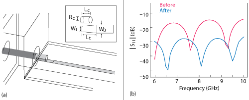
Figure 4 3D view of modified SMA-microstrip transition (a) and simulation results (b).
The SIW filter has low radiation loss and is easily integrated within a shielded enclosure. Because the filter’s metallic cavity is part of the ground system, the metallic framework of the enclosure makes direct contact, greatly simplifying its design. A sixth order fundamental mode SIW filter with a compact square cavity is used to achieve a good image-rejection ratio (IRR). Figure 5a shows the topology and its dimensions are provided in Table 2. Measured results agree closely with simulation, exhibiting a low VSWR in the passband from 8.2 to 9 GHz and meeting system requirements with a high IRR below 7.8 GHz (see Figure 5b).

Figure 5 Fundamental mode RF filter with square cavity: structure (a) and response (b).
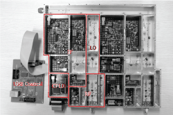
Figure 6 Assembled receiver front-end connected to the control board.
IF Link
The use of an external LO is feasible for a massive MIMO system. This eliminates sources of phase noise due to the LO module, especially in a TDD system, such as the power supply and reference signal distortion. Due to its relatively high linearity and large dynamic range compared with an active mixer, a passive mixer is used to convert RF signals to IF. It requires an LO as high as +17 dBm, so an amplifier with high P1dB is chosen.
The IF link is composed of four main component types: IF amplifiers, IF filters, digital control attenuators and switches. Sufficient IF gain is assured with five amplifiers in each channel. When a channel is turned off, the system removes power to all five amplifiers in the chain for power savings and isolation enhancement. Automatic gain control ensures sufficient dynamic range. This is realized by arranging the five IF amplifiers with two digital controlled attenuators in the proper order. The IF stage achieves 63 dB of gain control with 0.5 dB per step. In this way, the IF output is adjusted with changing input.
The IF filters suppress adjacent channel interference and spurious caused by nonlinear components such as mixers. One filter is realized with a stepped-impedance resonator (SIR) structure while the other two are constructed using lumped elements.
Two switches in each channel further enhance isolation between RF and IF ports when a channel is turned off. Test result shows that each switch provides isolation greater than 60 dB.
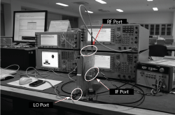
Figure 7 Dual-channel X-Band receiver being tested.
Other Modules
For practical considerations, the power interface uses only one 6 V power supply. The power module converts this to other voltages needed by the system and supports “hot plugging.” All control signals such as AGC and channel on/off are generated by a single-chip complex programmable logic device (CPLD) and each channel can be controlled separately through the CPLD-to-PC interface. Along with other protection circuits, the control module also determines the power up/down sequence of all the transistors and chips in the system.
To avoid potential interference between PCB modules and to meet EM shielding requirements, the total circuit is assembled within a single metallic housing with separate compartments. In the RF stage, absorbing material is also used. Figure 6 is a photograph of the assembled receiver front-end with the cover removed.
Implementation and Measurement
All circuits are fabricated on single-layer Rogers 4003C substrate material with a dielectric constant of 3.55 and thickness of 0.508 mm.
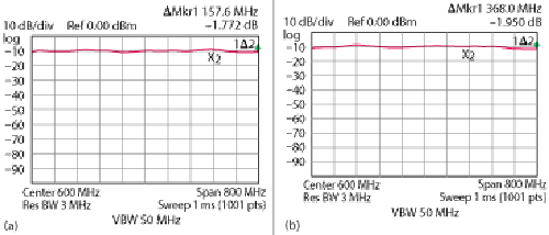
Figure 8 Channel 1 (a) and Channel 2 (b) gain variation.
Figure 7 is a photograph of the fabricated receiver front-end in the test environment, including a signal generator, signal analyzer, noise figure analyzer, network analyzer and PC to control the receiver front-end.
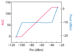
Figure 9 Receiver front-end AGC control and output power.
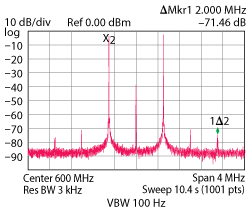
Figure 10 Measured receiver linearity.
In order to measure conversion gain, Keysight PSG E8267D and E8251A signal generators provide the LO signal and a single tone RF signal that is swept across the 800 MHz channel bandwidth. The IF signal is connected to a Keysight N9020A MXA signal analyzer. Test results (see Figure 8) show a maximum gain fluctuation of less than 2.1 dB with different AGC values over the 800 MHz frequency bandwidth of both channels.
The receiver must provide a stable output at baseband over a wide range input power. This is shown in Figure 9. With the AGC under PC control, output power is nearly constant at around -10 dBm while the input power of RF signal changes from -38 to -101 dBm. The input 1 dB compression points of these two channels are -25.8 and -26.1 dBm, respectively.
Linearity is tested using a two-tone signal with 1 MHz spacing and an input power of approximately -70 dBm (see Figure 10). Third-order intermodulation distortion remains less than -70 dBc up to an output power of 0 dBm.
Noise figure is measured with a Keysight N8975A noise figure analyzer. Noise figures for both channels are less than 1.8 dB with a minimum value of about 1.2 dB (see Figure 11). Due to the response of the RF bandpass filter, there is some deterioration near the band extremes.
Input return loss, measured with the Keysight N5230A PNA-L series network analyzer, is shown in Figure 12. Both channels are better than -12 dB, however, the measured results are worse than simulated (see Figure 4b). This may be due to several reasons such as errors in the active device model used for simulation and manufacturing tolerances of the connector interface.
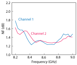
Figure 11 Measured receiver noise figure.
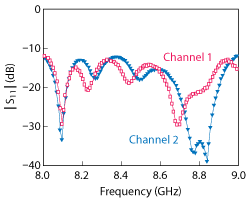
Figure 12 Measured receiver input match.
Finally, error vector magnitude (EVM) is used to quantify front-end performance using a representative input. The RF test signal is a standard TDD-LTE signal generated by the N7625B Signal Studio software. The symbol rate is 10 MHz limited by available test equipment. In addition, the front-end is switched continuously between its on and off states controlled by the E4438C signal generator. Using the model 89600A vector-signal-analyzer (VSA) software, with -70 dBm input power at the receiver front-end’s RF port, the measured EVM level is less than 1.4 percent, and a clear constellation is achieved while the output power in the occupied band is around -10 dBm. This can be seen in the error summary table of Figure 13.
Conclusion
A high performance dual-channel, X-Band receiver front-end demonstrates suitability for use in a MIMO system for future high speed communications or for phased array applications. The RF center frequency is 8.6 GHz with a 600 MHz IF and an 800 MHz bandwidth. Noise figure is less than 1.8 dB. Maximum conversion gain is 93 dB with 63 dB of gain control. The two channels are well matched with a passband gain variation of less than 2.1 dB.
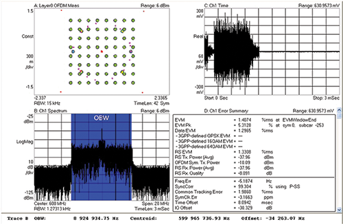
Figure 13 Constellation diagram, spectra and error summary of the MIMO test signal.
References
- Z. Yu, J. Zhou, J. Zhao, T. Zhao and W. Hong, “Design of a Broadband MIMO RF Transmitter for Next-Generation Wireless Communication Systems,” Microwave Journal, Vol. 53, No. 11, November 2010, pp. 22226.
- Z. Yu, J. Zhou, L. Zhao and L. Dai, “The Design of a 6 GHz Band RF Receiver with Excellent I/Q Image Suppression,” International Conference on Microwave and Millimeter Wave Technology, May 2012, pp. 124.
- Z. Chen, W. Hong, J. Zhou and J. Chen, “Design of Miniature RF Transceivers for Broadband MIMO Systems in Ku-Band,” Microwave Journal, Vol. 55, No. 11, November 2012, pp. 1082118.
- E. G. Larsson, O. Edfors, F. Tufvesson and T. Marzetta, “Massive MIMO for Next Generation Wireless Systems,” IEEE Communications Magazine, Vol. 32, No. 2, February 2014, pp. 1862195.
- P. J. Meier, H. C. Okean and E. W. Sard, “Integrated X-Band Sweeping Superheterodyne Receiver,” IEEE Transactions on Microwave Theory and Techniques, Vol. 19, No. 7, July 1971, pp. 6002609.
- A. Gustafsson, M. Alfredsson, M. Danestig and R. Malmqvist, “A Fully Integrated Radar Receiver Front End Including an Active Tunable Bandpass Filter and an Image Rejection Mixer,” Asia-Pacific Microwave Conference, December 2000, pp. 992102.
- A.M. Madni, P.T. McDonald, R.K. Hansen and L.A. Wan, “High-Dynamic-Range Airborne Tracking and Fire Control Radar Subsystem,” IEEE Transactions on Microwave Theory and Techniques, December 1989, pp. 194221948.
- N. Billstrom, “Compact Receiver Module for X-Band Radar Applications,” 33rd European Microwave Conference, Vol. 3, October 2003, pp. 112721130.
- J. Shefer and G. S. Kaplan, “An X-Band Vehicle-Location System,” IEEE Transactions on Vehicular Technology, Vol. 21, No. 4, November 1972, pp. 1172120.
- D. Gupta, D.E. Kirichenko, V.V. Dotsenko and R. Miller, “Modular, Multi-Function Digital-RF Receiver Systems,” IEEE Transactions on Applied Superconductivity, Vol. 21, No. 3, June 2011, pp. 8832890.
- J. Wong, R. Dunnegan, D. Gupta, D. Kirichenko, V. Dotsenko, R. Webber, R. Miller, O. Mukhanov and R. Hitt, “High Performance, All Digital RF Receiver Tested at 7.5 Gigahertz,” Military Communications Conference, October 2007, pp. 125.