
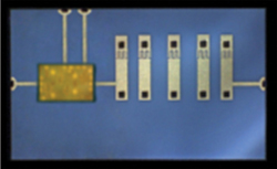
Figure 1 Thin film/GaN integration.
Recent marketplace realities have included looming budget cuts, competition with low-cost competitors and regular large program contract delays, all highlighting the increasing importance of versatile, configurable, reusable RF modules and hardware. Size, weight and power (SWaP) innovation and wider bandwidth, multimode, smaller platforms are the mantra.
Recent Filter Innovations and Market Drivers
The history of advances in the development of RF and microwave filters is well documented, and broad innovation goals have remained essentially the same over decades. Better performance, smaller size, lower cost and greater power-handling are some of the general “wants” engineers are always working to achieve. However, certain observations about recent industry trends can be made. For instance, filter innovation in the last 10 years has been spurred by material advances and ever-increasing electromagnetic simulation speeds and capabilities. Accordingly, lumped component products are supporting higher power-handling, cavity filters are shrinking in size/volume (by a factor of two or more) with little loss of Q, tunable filters are achieving higher power-handling at smaller sizes and low passive intermodulation (low PIM) products are being cost-effectively manufactured in higher volume.
The industry has observed the following trends:
- Ceramic material advances, particularly specialized material consistency, have facilitated higher yields on ceramic resonator filters and on higher-performance ceramic substrate printed filters. Additionally, advanced ceramic materials have made dielectrically-loaded waveguide super high Q filters possible. Single-, dual- and triple-mode “puck” filters provide better performance at a smaller size.
- Newly developed materials or substrates that enable practical thin film filter implementation are equally at home supporting GaAs and GaN bare-die integration, allowing further size reduction in multifunction module construction. As an example, Figure 1 shows a BSC product with GaN integration on thin film.
- In addition to virtual prototyping of various innovative mechanical realizations, 3D modeling and printing and other computing advances have allowed more complex phase, delay, and matching criteria in specifications, as well as in real-time testing and verification.
- System computing technology has expanded possibilities for filtering cancellation techniques, driving some agile filter technology. Various methodologies have been tried, with mixed results. Standard techniques and components like varactor diodes cannot handle the system power requirements. Millions of dollars have been invested in novel agile materials that remain unproven. High power pin diodes have filled some voids, but much work remains. MEMS technology has not yet effectively aided band tuning/agility.
- High-frequency MMICs shrink cost and size of various filter assemblies, for example, up/down-converters, making them increasingly filter-dependent in terms of size and cost, adding to pressure for filter design innovation in commercial and military arenas.
- Commercial and military system frequency spectrum overcrowding has vastly increased demand for notch filters, simultaneously escalating demand for size and performance improvements in band-reject realizations.
- Even with spectrum interferers addressed, the push for greater speeds, more data and more connected users has created the need for low PIM systems and low PIM test equipment. PIM is directly related to noise, noise to bandwidth and bandwidth to supportable speed.
- Cavity-like performance and Q are being sought in surface mount formats.
- Amplifier semiconductor materials have lowered noise figures, allowing higher filter insertion loss to be traded for smaller filter size while maintaining overall system cascaded noise.
Against the backdrop of these broad trends, innovation in filter design and the usage of specialized filter products continues. Military and commercial telecommunications, along with certain medical industry technologies, prompt advances in materials, packaging, design and arrangement of filters to meet key market challenges. This article focuses on five current innovative approaches to address present and future market needs.
Thin Film Approach to Miniaturized RF Integration
Traditional thin film microwave hybrid circuit designs have declined in many applications, displaced over the years by the evolution of MMICs and the development of low-cost packaging. These advances enabled active microwave design to be realized on soft-board materials at frequencies above 60 GHz. More recently, the advent of special ceramic materials has facilitated the realization of high-performance miniature filtering using thin film, enabling the integration of such filtering into multifunctional subsystems.
While many thin film circuits have featured a degree of filtering as an adjunct, until the development of modern substrates, thin film was not widely regarded as a suitable technology for high-performance miniaturized filters. Alumina substrates could not be readily exploited for filtering applications due to low filter Q, relatively poor thermal properties and an εr yielding impractical size and relatively poor selectivity.
On the application side, SWaP reduction remains critical, particularly in the UAV and space environments. Modern information gathering and distribution systems are tending toward greater dependence on small airborne platforms in military and civilian contexts. A plethora of fixed and rotary-wing vehicles are affordably available in a wide variety of shapes and sizes, creating opportunities for military and commercial enterprises alike.
With greater dependence on RF systems for control, navigation and telemetry, the proportion of payload size and weight allocated to RF modules is significant, especially when factoring in the usual complement of EW and ECM equipment found onboard military UAVs. Smaller, lighter and more efficient onboard systems extend the mission time and capabilities of the craft. SWaP considerations are fundamentally important in the realm of spacecraft systems, and with the widespread use of RF technology in space, cost-per-kilogram to achieve orbit and the small form factor of modern satellites dictate that “smaller and lighter” is always better.
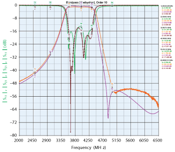
Figure 2 Measured 4 GHz bandpass response (orange/green) against simulation (purple/red).
Analysis of the size and weight composition of RF systems shows that two key aspects contribute significantly: discrete RF filters and the inherently modular construction of subsystems. Clearly, shrinking filter size and integrating further would offer discernible advantages. The challenge is that filter size is limited by the laws of physics. Common dielectrics, such as air or PTFE, produce relatively large resonators and cavity volume, while integration of self-contained machined housings, often from different manufacturers, can be far from seamless or space-efficient.
Comparing volumes, a typical 8-section lumped element filter at 2 GHz might be 2.0" × 0.6" × 0.4" in size, and an equivalent air cavity combline would be even larger at 5.9" × 1.8" × 0.9". A thin film approach drastically reduces size to about 0.4" × 0.4" × 0.14" (including cover). This reduction in size is facilitated by the high dielectric constant of the ceramic substrate base, typically featuring an εr of more than 25. The unloaded Q of interdigital and combline structures realized in thin film is in the range 250 to 400. By comparison, conventional lumped element and capacitively-coupled ceramic coaxial resonator devices have Q values of 50 to 300 and 300 to 600, respectively. In many cases, thin film offers comparable selectivity.
The design process starts by forming a transmission line model, developing the filter order and preliminary physical layout required. This simplistic model uses a homogenous distribution of the substrate’s dielectric properties and simple conductor parameters to speed initial development. The next step is to import the result from the transmission line model into a Finite Element Analysis (FEA) package. At this stage, the virtual prototype can be modelled in detail, including auxiliary parameters such as conductor surface roughness and parasitic effects. The simulation takes into account the inherent coupling between non-adjacent resonators that forms a transmission zero on the high side of the filter passband in interdigital and combline designs, as shown in Figure 2. Edge vias are then matched into both the filter and the interfacing transmission lines.
After the FEA process, the optimized filter geometry is assembled onto photolithographic masks and developed onto laser-drilled, gold-sputtered substrates. Surface conductor thickness of typically 5 µm maintains an adequate multiple of skin depths to achieve optimum conductivity. Depending on the application, thin film devices can be interfaced by soldering or bonding, mounted by reflow or conductive epoxy, enclosed in self-contained shielding or channelized. In mass production contexts, thin film devices are ideally suited to pick-and-place assembly processes.
Such flexibility and miniaturization allows conventionally large filter-based modules – for example, switched filter banks or pre-selectors, in which filtering accounts for most of the volume and mass – to be drastically reduced in size. The ability to realize filter structures on the same conductor plane as other components in the RF chain obviates the need for discrete filter packaging, connectors or glass-to-metal seals and eliminates associated discontinuities.
Newly developed substrates enabling practical thin film filter implementation are equally suitable for GaAs and GaN bare-die integration, allowing further size reduction in multifunction module construction. Given the advantages, it seems likely that integration of active components and passive filtering will become more commonplace in future module design (see Figure 1).
New TEM Structure for size Reduction
Transverse Electromagnetic (TEM) mode structures in the form of resonators have been a staple in RF and microwave filter design for decades. Recent innovations represent a significant improvement for certain applications. The primary innovation consists of a revised layout for TEM structure resonators that exploits total cavity volume to lower frequencies with only minimal Q degradation. With this new approach, overall filter volume is significantly decreased. Newly devised coupling methods achieve wider percentage bandwidths, along with elliptical responses in the real and imaginary domains.

Figure 3 90 MHz bandwidth filter data.

Figure 4 1 MHz bandwidth filter data.
Figures 3 and 4 show measured results for filters with 90 and 1 MHz bandwidths. The first has nine sections, and the second has four. Corresponding filter dimensions are 5.0" × 5.0" × 2.5" and 3.2" × 3.2" × 2.2", respectively.
Lowering the frequency of operation without drastic degradation of unloaded Q is particularly advantageous in the VHF to UHF frequency range. With bandwidth limitations almost removed, relative bandwidths ranging from 0.5 to 40 percent have been realized. In addition to smaller bandpass filters, cavity size reduction enables compact band-reject filters with small footprints and high performance. The TEM structure supports high power applications typically associated with the UHF to VHF frequency range. In essence, the classic TEM resonator structure has been rethought by eliminating the portions contributing only weakly to supporting electric or magnetic fields. The new structure is lighter and produces greater electrical length. Using this approach, a full 90 percent of band-reject filter volume arises from the volume of the resonator cavities, compared to a much lower percentage in the classic case.
Thin Film Lumped Component Filters
An innovative and versatile thin film lumped element approach supports highpass, lowpass, bandpass and notch designs using the same basic structure, simply by removing or reconfiguring specific components. The resulting filters exhibit broad spurious-free stopbands, small physical size, excellent amplitude and phase match and high reliability due to the thin film construction.
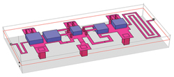
Figure 5 CAD representation of thin film lumped component filter.
Thin film microstrip filters are important components in modern hybrid integrated subassemblies. For filters in such applications, subsystem designers often use edge-coupled, commensurate line, hairpin and other well-known distributed topologies. Distributed topologies, however, have certain limitations. Constructing broadband distributed filters in conventional microstrip is challenging due to the large impedance ratios required, and realizing elliptic responses exhibiting finite transmission zeros in distributed networks is difficult. At lower microwave frequencies, the physical size of distributed filters is relatively large. Finally, distributed filters by their nature present challenges for realization of broad stopbands free of spurious responses.
Lumped element microwave filters address many of these limitations, but present difficulties of their own when used in thin film assemblies. Lumped component filters are usually constructed using parallel plate chip capacitors and air-wound inductors soldered into a small housing. Skilled manual labor is required to build and tune such filters. While the volume occupied is small compared to distributed counterparts, it is often difficult to integrate lumped component filters into an otherwise all thin film assembly.
At microwave frequencies, a hybrid lumped/distributed structure is an excellent solution enjoying the best of both worlds. Typical construction consists of an alumina carrier, single layer caps and printed inductors. Possible end launches include coplanar with edge wraps, coplanar with filled vias and microstrip.

Figure 6 Measured response of hybrid thin film lumped component filter.
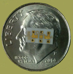
Figure 7 Microminiature 5.83 GHz C-Band filter.
A hybrid C-Band filter was designed and manufactured to demonstrate the feasibility, size and performance advantages of this approach. Figure 5 shows the CAD representation of the 5.83 GHz filter producing the measured response shown in Figure 6. Figure 7 shows the relative physical size of the 5.83 GHz filter, which is approximately 0.26" × 0.13" × 0.1".
Expanding 4G/LTE Filtering Solutions
The ongoing 4G/LTE rollout’s emphasis on increased data transmission and resolution of co-location issues for signal types ranging from earlier generation cellular to GPS have made the testing of supporting components ever more critical and challenging. Commercial telecommunication applications mandate full testing and understanding of the performance of virtually every component in a device or system.
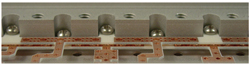
Figure 8 K&L's patented low PIM high power series capacitor.
Special filtering solutions simplify testing and can, in some cases, make seemingly impossible tests relatively easy. In response to customer needs, various test scenarios have been developed utilizing custom filters that increase dynamic range. These test setups employ filter building blocks and technologies, such as a patented low PIM capacitor and complex multiplexers and tunable filters with adjustable bandwidths.
Conceivably, individualized “brute force” PIM distortion testing in the LTE frequency bands could require large numbers of individual fixed frequency filters due to the number of LTE frequency and bandwidth combinations. Two recently-developed adjustable bandwidth tunable filters capable of tuning both bandwidth and center frequency could replace as many as 105 fixed frequency filters.
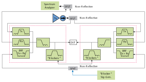
Figure 9 4G/LTE test setup.
Specialized Filters and Test Configurations
The highpass/lowpass duplexer is a basic filtering element in many test setup schemes. While the lowpass filter can be made of one piece for low PIM purposes, the highpass construction poses a great challenge. Multiple solder joints and dissimilar metals can be intermodulation sources, directly impacting the dynamic range of the system. In June 2014, K&L Microwave was awarded US Patent 8742869 B2 for the low PIM high power series capacitor shown in Figure 8. This paved the way for various broadband low PIM and wideband structures.
Ultimately, testing of components for use in 4G/LTE systems requires input of the planned transmit (Tx) frequency simultaneously with “blocker” signals applied in virtually any input/output combination. Figure 9 shows a test configuration that allows the engineer to input the appropriate Tx signal along with any blockers required. The setup permits Tx and blockers to be swapped from input to output ports of the device under test (DUT), and supports forward and reverse measurement of DUT performance without moving any connections or cable locations.
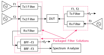
Figure 10 Triple beat test configuration.
One of the most difficult tests required in today’s environment is the “triple beat” test. Three frequencies are simultaneously injected into the DUT. Two are typical uplink, or Tx, frequencies that could be experienced by the device in normal operation. For this particular test, these two signals are spaced just 1 MHz apart, so that they occur in a single channel. The third signal is a blocker from the receive (Rx) band, simulating interfering signals that may be encountered in actual operation.
Traditionally, this test is set up using isolators to protect the amplifiers, hybrid quadratures to combine the signals, filtering to clean up injected signals and attenuators to protect the spectrum analyzer’s input. Isolators potentially create additional spurious frequencies that are not part of the test, while the hybrid quadratures require amplifiers to provide 3.5 dB of additional power. Further, the attenuators directly reduce the dynamic range of the spectrum analyzer. Taken together, these factors significantly reduce the test setup’s effectiveness.
Figure 10 shows a test configuration that eliminates most of the issues associated with the typical triple beat test setup. A “standard” Tx/Rx diplexer is used at the output to terminate the injected Tx signals and as an injection port for the blocker in the center of the Rx channel. The Rx channel of the input triplexer then feeds the test signal to a bandpass/bandstop diplexer on the path to the spectrum analyzer. This diplexer has both the bandpass and bandstop filters tuned to the blocker frequency. The bandstop portion of the diplexer passes the test signal to the spectrum analyzer while removing the injected blocker signal. The blocker signal is properly terminated at the output of the bandpass port. This configuration provides clean signal paths with little to no spurious interferers created by the test setup.
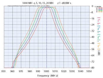
Figure 11 Tunable bandwidth capability of adjustable bandwidth filter.
In addition to proper termination of injected signals, this configuration offers another advantage related to the return loss of the filters and reduction of reflected signals. With 20 dB return loss at each of the filter ports, reflections back into the test environment are minimized. In other setups, reflections from test components create uncharacterized spurious signals that introduce uncertainty. Further, proper termination of all injected signals improves the dynamic range of the overall system. Now Tx signals, terminated through diplexers or triplexers, have no opportunity to reflect into the system and mix with others, creating potential problems. Injected blocker signals terminated before the spectrum analyzer minimize any mixing that might take place inside the analyzer. This configuration provides a clean and reliable setup.
Tunable Devices with Adjustable Bandwidths
While the testing of many components is best accomplished with multiplexers, some device specifications require a single filter to provide a clean signal to the test system. In such cases, vast numbers of individual filters can be required because of the number of LTE frequency and bandwidth combinations. An “adjustable bandwidth tunable filter” can be an effective alternative to minimize the number of fixed frequency filters for reduced space, greater utility and lower cost. Figure 11 shows plots for a filtering solution that tunes both its bandwidth and center frequency. Two of these filters will cover any bandwidth from 5 to 20 MHz and any center frequency from 700 to 2700 MHz. The figure shows the variable bandwidth capability at 1000 MHz. Two digitally-controlled filter assemblies of this kind could replace as many as 105 fixed frequency filters, simplifying testing and reducing cost.
Mitigating Self-Generated Interference
Self-generated communications interference is a problem faced by many RF and microwave communications customers. Recent tunable filter advances are mitigating past problems and enhancing future systems. Examples of recently introduced solutions are:
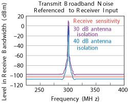
Figure 12 Typical spectrum of a transmitted signal.
- Microwave digital high-speed (< 100 ns) voltage-tuned agile filters extending into S-Band (with coverage through X-Band planned) in miniature, reflowable SMT packages.
- Highly integrated filter products with significant SWaP reduction compared to legacy filters that maintain 5 W in-band power over the entire military tactical radio tuning range in single- and dual-channel configurations.
- Mini SMT bandpass filter options from 30 MHz to 3 GHz.
- Narrowband and wideband interference cancellers, some of which do not require an interferer reference, thereby enabling cancellation of off-platform interferers.
- Deep notch filters to create communications channels in wideband, high power signals.
- Miniature, lightweight (0.5 lb) filter and power amplifier cascades for co-site interference issues inherent in UAV retransmission applications.
Military Radio Co-site Interference Mitigation
Military radios often operate in close proximity to additional radios, giving rise to co-site interference. Military radios must be able to operate in severe co-site interference environments. Figure 12 shows a typical spectrum of a transmitted signal evaluated at the co-site receiver input location over the receive bandwidth under two conditions of co-site transmit-to-receive antenna isolation, 30 and 40 dB. The receiver sensitivity superimposed on the chart represents the minimum signal required for acceptable demodulation in the receiver. Antenna isolation of 30 dB yields a broadband noise level that exceeds the sensitivity level of the receiver over the entire band. Hence, weak or distant signals within the receiver’s inherent capability would be “lost” in the noise created by the co-site transmitter.

Figure 13 Basic Maxi-Pole® filter selectivity.
Greater isolation can effectively be achieved through the use of selective filtering at the transmitter to minimize broadband noise. Selective filtering is applied following the primary noise sources in the transmit signal chain, having the overall effect of lowering the broadband noise without necessitating an increase in antenna isolation.
As an example, a 2 percent instantaneous 3 dB bandwidth Maxi-Pole® filter with the tuning range of 90 to 200 MHz would have an insertion loss of approximately 5 dB (4.8 dB actual). This selectivity characteristic is shown in Figure 13. For greater selectivity, multiple filters can be placed in cascade with low noise amplifiers (LNA) for inter-filter isolation and filter loss recovery, followed by a power amplifier designed for efficient operation and low noise output. Figure 14 shows three filters in a cascade with LNAs and a power amplifier for enhanced broadband noise performance. The noise performance of this arrangement, referred to as Integrated Cosite Equipment (ICE) at Pole/Zero, is 20 to 40 dB superior to the transmitter for measurements taken more than 4 MHz from the transmit carrier.
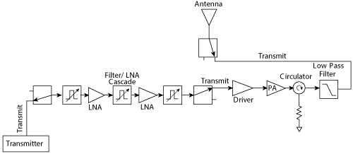
Figure 14 Transmit filtering block diagram.
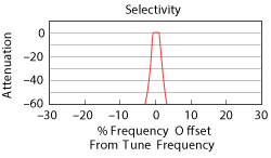
Figure 15 Selectivity characteristic of a transmit filter/LNA cascade.
Figure 14 shows a technique to mitigate co-site interference, decrease transmitter spurious output and increase output power available from the transmitter. Figure 15 shows the additional selectivity achieved.
Multiple transmitters coupled to antennas in close proximity create a condition called reverse intermodulation, characterized by the coupling of energy from one transmitter into the antenna of another, creating a simultaneous flow of reverse and forward energy. Coupled energy mixes in the nonlinearities in the output network of the transmitter to create an infinite number of intermodulation products. The products are then re-propagated to the collocated receivers, creating products of sufficient level to preclude reception at those frequencies. Thus, a co-site transmitter’s output carrier signal can significantly degrade the performance of the receiver.
The 1 dB compression point of an amplifier is the actual output power where the small signal gain extrapolation exceeds the actual gain by 1 dB. For co-site communications analysis, this concept is modified to accommodate the variation in this parameter due to the presence of selectivity in the system and the effect of multiple inputs to the receiver. The compression characteristics of a receiver are evaluated prior to detection with a desired signal 1 dB above sensitivity level. An interfering signal at various displacements from tune frequency is increased in amplitude until the desired signal degrades to the sensitivity level. This level is designated as the 1 dB desensitization point and is representative of the debilitating effect the interferer has on the desired signal. The red curve in Figure 16 represents this characteristic for a typical receiver.

Figure 16 Receiver 1 dB compression characteristics.
While a 1 dB drop in system gain is seemingly subtle, empirical evidence suggests that as the interferer increases above the 1 dB desensitization point, it is not uncommon for the desired signal level to drop as much as 4 dB for every increase of 1 dB in interferer.
The use of a receive filter or filter/LNA cascade similar to that used in the transmit chain can create “preselection” of the energy from the receive antenna and reduce the relative level of the co-site interferer to the desired signal. Figure 17 shows the same filter/LNA cascade from Figure 14 configured for receive operation. The net effect of this level of preselection is shown graphically by the blue curve in Figure 16. Under this condition, the debilitating effect of co-site interference is mitigated by the selectivity of the preselector.
As in the transmit environment, nonlinear effects in the receive chain can be the source of additional co-site interference. The preselection filter serves to minimize the level of the interfering signals prior to the receive nonlinearity, thereby minimizing any resulting products created within the receiver.
CONCLUSION
The Microwave Products Group (MPG) has established an Engineering Innovation Council comprised of senior design professionals from all four business units. Some of the new technologies and inventions in this article are direct results of that collaboration. Anticipating future requirements after an extensive review of the current state of technology in the RF and microwave community, the MPG R&D and engineering teams are actively applying their collective expertise to developing tomorrow’s products. MPG welcomes opportunities to leverage an evolving technology roadmap to meet customers’ immediate and emerging communication and signal control needs.
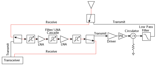
Figure 17 Half duplex Tx/Rx integrated co-site equipment.
Certain aspects of the innovations presented in this article represent the intellectual property of MPG’s parent Dover Corp. and are protected by patents, pending patents and information filings on these proprietary rights.
Acknowledgment
The authors thank Kevin W. Asplen for his help preparing this article.