Editor’s Note: The quest for interoperability between RF/microwave EDA tools goes back to at least 1987 and the DARPA program known as MIMIC. This program launched a study to find the best way to produce reliable, high performance MMICs through the “development of computer-aided design capabilities.” CAD companies teamed with IC manufacturers to develop standards for file formats allowing the exchange of data across platforms and design environments. Today, interoperability extends to nearly all software-based design tools including circuit/system schematic-based environments, physical layout, EM simulation, multi-physics, manufacturability and test systems, taking into account software from multiple vendors and supporting enterprise design flows. A new age is upon us whereby EDA providers are collaborating with each other to streamline design flows through interoperability and design automation. This improved functionality allows engineers to be more productive than ever before. The following is an update on the latest developments in interoperability and the impact on design.
Keysight Technologies
Keysight’s workflow environments provide a way to simulate, measure and analyze components and systems in a variety of applications. This is made possible by focusing on software interoperability across electronic design automation (EDA) tools as well as measurement application software for specific test needs. As a component or device moves through its lifecycle—from early design all the way to volume manufacturing—customers can achieve greater confidence in their designs, products and schedules.
In recent years, the need for greater interoperability between design tools has intensified due to two main trends. The first is a general movement from single-technology designs to those that incorporate multiple technologies within ever-smaller enclosures. This leads to many challenges, and one of the most difficult is the potential for coupling between the subsystems within the device. Solving these problems quickly and efficiently depends on circuit simulators, electromagnetic (EM) simulators and layout tools that are designed to work together.
This leads to the second trend: the need for greater efficiency in the design flow. In many industries, headcounts and budgets are shrinking as competitive pressures drive shorter design cycles. If team members are using differing tools, they may need to convert or translate designs from one format to another—and this may cause inefficiency and errors.
Several years ago, Open Access was introduced as a common database for custom IC design. Keysight adopted this database in its flagship simulation platform, Advanced Design System (ADS), and its EM simulation tools. Today, ADS 2014 provides several new features that increase interoperability and address the two main trends described above. As an example, ADS 2014 goes beyond the use of a common database for circuit and EM simulation. To help designers save time—and eliminate hundreds of mouse clicks—the software includes automatic EM simulation set-up and design partitioning. This automates the process of removing SMD and IC active devices and replacing them with EM ports in the design layout.
Another addition is a next-generation PCB integration solution – the ADS Board Link (ABL). This provides a bidirectional interface to enterprise PCB tools, enabling ADS to import layouts, schematics and libraries. ABL also enables easy transfer of RF schematic and layout designs started in ADS, to enterprise PCB environments for integration into a larger design for floor planning, modification to accommodate physical design constraints, and exportation back to ADS for verification.
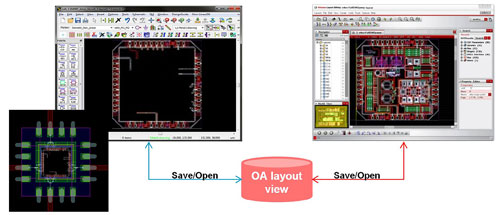
Figure 1 Advanced Design System 2014 uses the Open Access database, enabling bidirectional schematic interoperability with Cadence Virtuoso.
Designers of silicon RFICs can now use ADS 2014 to simulate a design from Cadence Virtuoso with no importing or file translation required because both tools use the same database (see Agilent’s article, p.66 in this issue for more about the benefits of this interoperability). For those making measurements with the latest Keysight instruments, ADS 2014 provides enhanced links through an upgraded Command Expert Mode in its Connection Manager (see Figure 1).
In today’s design cycles, interoperability extends beyond EDA tools to include information sharing between software and hardware as well as interoperability across multiple hardware platforms. Incorporating multiple radios into less space also adds new challenges to device testing. The difficulties grow when those radios use sophisticated multiplexing and transmission schemes such as MIMO, space/time coding, beam-forming and carrier aggregation.
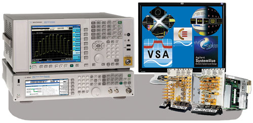
Figure 2 Benchtop and modular vector signal generators and analyzers leverage common measurement algorithms that represent building blocks in their measurement.
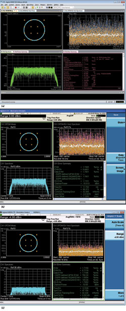
Figure 3 These three traces show the same LTE measurement made with the 89600 VSA software, (a) an MXA signal analyzer running X-App VSA software (b) and a modular PXI VSA with X-Apps software (c).
As a product moves along its lifecycle, testing requirements evolve from “unbounded” in R&D to “just enough” on the production line. Satisfying those needs while also addressing business drivers often requires an optimal combination of benchtop and modular test equipment. The benefits grow if the platforms are well harmonized and the associated measurement software provides consistent results.
The availability of compatible benchtop and modular solutions provides the fastest path to a completed design and the lowest total cost-of-test (see Figure 2). It also reduces the risks inherent in the product lifecycle. As an example, Keysight offers a common suite of signal-generation and signal-analysis software that can be used across its benchtop and modular signal generators and signal analyzers. This enables engineers to easily correlate test results between the development and manufacturing phases.
Specific to signal analysis, Keysight provides a range of capabilities. This starts with basic functionality in the form of spectrum and “power suite” applications for all stages of product development and manufacturing. The next level comes from X-Series measurement applications, which offer capabilities such as power, harmonics, spurious and phase noise across benchtop and modular instruments. For advanced modulation analysis, the Keysight 89600 VSA software is compatible with—and provides consistent results from—a wide range of Keysight measurement platforms (see Figure 3).
NI/AWR
AWR Corporation, a National Instruments Company and leader in high-frequency EDA software, has had a long-standing commitment to provide design engineers with access to best-in-class, third-party tools through integration with the AWR Design EnvironmentTM. The AWR ConnectedTM family of products supports the flow of data between high-frequency design software from AWR and products from third-party software and hardware manufacturers automating the exchange of design and simulation/measurement data from software-to-software and/or software-to-hardware design environments. Design domains addressed include printed circuit boards, test and measurement (T&M), as well as MMIC thermal and related synthesis technologies.
To keep pace with evolving engineering challenges and new tools on the market designed to address these issues, AWR has recently added several important interoperability links to its AWR Connected product line. These links provide interoperability to various tools for specific analyses (i.e. EM, thermal), complex physical structures and design flows and provide engineers with an opportunity to address specific engineering issues while utilizing existing design information.
In a significant development, AWR and ANSYS Inc. recently announced their efforts to integrate ANSYS® HFSSTM, a leading 3D EM analysis tool, into Microwave Office. With this design flow, Microwave Office users can readily access HFSS for analysis of EM fields and coupling of 3D structures like bumps, bond wires, pins, tapered vias and ribbons, which are essential to successfully designing and realizing microwave circuits like monolithic microwave integrated circuits (MMIC), densely-populated RF circuit boards and multifunction modules.
The link between the two software tools is accomplished through the use of AWR’s EM SocketTM open standard interface, which enables AWR users to access a broad range of electromagnetic (EM) tools from within the Microwave Office design environment. It is this same feature that also enables AWR Microwave Office users to essentially simulate EM structures with a single mouse click using either AWR’s AXIEM® 3D planar method of moments solver or AnalystTM 3D finite element method EM software.
In addition to enabling ANSYS HFSS 3D EM simulation capabilities from within the NI/AWR Design Environment, the connection allows the resulting 3D layered format exported from the EM Socket interface to connect to the ANSYS multiphysics portfolio. That suite includes ANSYS SIwave® for signal/power integrity analysis and ANSYS Icepak® for thermal characterization.
High-power RF components not only produce high power—they also generate heat. This makes it important to not only understand the electrical performance of the end device but also the impact of its thermal profile. In addition to the link to
ANSYS Icepak for thermal analysis, AWR Connected now provides interoperability to CapeSym’s SYMMIC thermal FEM analysis software, which provides a co-simulation, software-to-software, electrical/thermal, MMIC design environment.
AWR Connected for SYMMIC is a unidirectional interface flow developed especially for high power monolithic microwave integrated circuit (MMIC) designers to enable them to easily take AWR’s Microwave Office high-frequency circuit designs into CapeSym’s SYMMIC software package for thermal analysis. Together, AWR & CapeSym provide high power RF designers with the ability to obtain optimal electrical performance with proper consideration given to thermal operating properties as well. This results in more robust and reliable next-generation RF and power systems.
In support of complex PCB layout design flows, AWR is also partnering with Cadence Design Corporation on a new and improved flow between AWR tools and Cadence’s Allegro board solution. It is not uncommon that the RF functions on a board occupy only a small footprint on the final overall PCB design. While this RF area may be small, the importance of getting the design right is paramount. Unfortunately, is it also quite typical that the RF layout is designed in isolation and later placed into the final design. When this happens, the RF performance often suffers. Therefore it is very desirable and beneficial to perform a verification simulation using the actual layout from the full production PCB tool before prototyping.
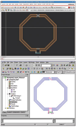
Figure 4 Layout of spiral inductor defined in Cadence Virtuoso imported into HFSS for 3D full-wave analysis.
AWR recognized this need several years ago and first partnered with Cadence in 2010 to provide the AWR Connected for Cadence Allegro design flow using Applied Computational Sciences (ACS) as the intermediary. This powerful solution is popular for an EM extraction flow taking data from Cadence and inputting it into AWR’s Microwave Office circuit design tool, where it can also be leveraged using AXIEM® for 3D planar EM simulation.
As EM simulation has matured and become much more a part of the front end design process, mutual key customers have been requesting a tighter, more robust solution. In response, AWR and Cadence began working together in 2013 to ensure model compatibility across tools. The result is a 3D printed circuit board (PCB) flow that takes the RF schematic and layout from Microwave Office and exports the data into Cadence format such that it can be quickly and easily read in, plugged into the overall PCB design, and simulated/verified.
ANSYS
ANSYS is equally committed to providing open integration of HFSS, an industry leading electromagnetic field simulation technology, with third party microwave circuit simulation and EDA design software packages. Such interoperability allows companies to create customized design flows to fit their needs. The key enabling feature supporting this integration is the new 3D Layout interface. HFSS 3D layout is ideal for designers who work in layered geometry found in monolithic microwave integrated circuits (MMIC), densely-populated RF circuit boards and multifunction modules, or layout of high-speed components, including on-chip embedded passives, IC packages and PCB interconnects. These types of designs can be easily modeled in the HFSS electrical layout environment or imported directly from leading design software packages such as National Instruments/AWR (described previously) and Cadence Design Systems (see Figure 4).
The HFSS 3D layout feature enables seamless integration with AWR’s Microwave Office and Cadence® Allegro®, APD, SiP and Virtuoso® allows RF, SI and digital engineers to set up ready-to-solve chip, package and board simulations from within the host environment. The easy-to-use capability is ideal for engineers who are not familiar with 3D electromagnetic modeling but require the rigor, accuracy, and reliability that HFSS provides. All the necessary HFSS setup steps (geometry, material properties, port setup, and boundary conditions) are easily and quickly applied in the AWR or Cadence interface (see Figure 5).
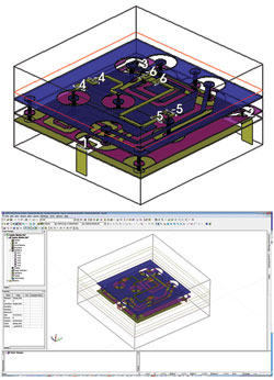
Figure 5 Layout of structure with defined ports originally designed in AWR imported into HFSS for 3D full-wave analysis.
Engineers can easily perform a direct setup of a Microwave Office, Allegro, APD, SiP or Virtuoso layout design that can then be analyzed with HFSS. Users simply specify which regions, or connected regions, are to be solved by HFSS by specifying a cutout region in the layout tool. Once the region has been defined, the appropriate nets are selected and ports are automatically assigned to the nets or solder balls in the design. To complete the setup, the user specifies the solution frequency and sweep range.
Once setup is complete, the 3D electromagnetic model is solved by the HFSS finite element electromagnetic solver. Since the solution region, nets of interest, excitation ports, and boundaries are automatically created and/or assigned in the layout, engineers do not need to be familiar with 3D modeling. Such integration provides access to HFSS while making model creation extremely simple and fast. Engineers obtain very accurate electromagnetic field simulations of high-speed differential pairs, via transitions, ball grid array transitions, package-to-PCB transitions, passives on silicon, RF circuits and more.
Once the imported geometry exists in HFSS, users can do further analysis beyond 3D full wave electromagnetics by leveraging the ANSYS® WorkbenchTM. The Workbench framework allows users to perform detailed multiphysics analyses on the same imported geometry. For example, the design of an RF power amplifier must now consider how the device’s thermal performance will impact the system’s overall frequency response. Optimal designs can be accomplished only when both issues — electromagnetic and thermal performance — are considered in an interdependent manner. Moreover, today’s microwave electronics systems are incorporated into demanding system-level environments. A power amplifier may be part of a phased array antenna that is mounted in a UAV that is expected to circumnavigate the globe. Vibration analysis is a critical component to this integration. What impact will in situ vibrations have on the antenna’s beam steering capabilities? Only an integrated multi-physics solution can provide the answer. The ANSYS Workbench delivers an innovative project schematic view that ties together the entire simulation process, guiding the user every step of the way. Even complex multiphysics analyses can be performed with drag-and-drop simplicity.
COMSOL
Simulation enables faster product development by providing key information about how a design will perform prior to the manufacturing of physical prototypes. For electrical engineers, ever diminishing component sizes on printed circuit boards, integrated circuits, and MEMS devices demand that greater and greater accuracy be obtained to correctly predict device performance and characteristics. To achieve this, the interactions of multiple physics must be combined and analyzed within one and the same simulation.
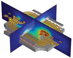
Figure 6 COMSOL now supports the ODB++ file format for importing such files and performing analyses on the PCB components they represent.
Take power electronics, for example; analyses of the performance of solid-state electronic devices must include far more than just a single physics type. In these devices, it is crucial to understand heat management processes in great detail. This requires that current conduction be coupled to heat conduction as well as to structural simulations to check for stress and deformation. When designing flexible printed circuit boards, such as those used in wearable devices, it is beneficial to have both a fast development cycle and a reliable product that is ensured by simulation. This entails ensuring that the circuit board can deform as intended and does not break after repeated deformation, a truly multiphysics analysis.
How is this done? Computer aided engineering (CAE) software requires strong interfacing and interoperability capabilities in order to leverage the strengths of different software. With the ECAD Import Module, an add-on to COMSOL Multiphysics, ECAD files can be imported directly into the COMSOL® software, where 2D layouts can easily be converted into 3D geometries for further analysis.
Within the COMSOL environment, multiple physics interactions can then be combined and analyzed including the electromagnetic, thermal, and structural behavior of components and devices. One new feature introduced with COMSOL Multiphysics version 4.4 is the ability to import ODB++files into the software (see Figure 6). “With ODB++import, the engineer is able to generate 2D or 3D geometry based on the layers of a circuit board. The geometry can be meshed and used together with any of the COMSOL modules for simulation,” describes Lorant Olasz, product manager for the interfacing products available with
COMSOL Multiphysics.
ECAD data can be imported using formats that contain layouts for the individual layers in a device such as a PCB or a chip. The ECAD Import Module, by recognizing the geometric components of a layout, will construct plane geometry objects from the files. These objects can then be extruded based on information (provided in the file or during import) about the layer stack-up. For IC and MEMS simulations, GDSII formats are supported. The NETEX-G, ODB++, and ODB++(X) file types can be imported for simulating PCBs. The NETEX-G format is the native file type for the program of the same name, which can extract connected metal traces from formats that are widely used for when PCB designs are sent for fabrication, such as drill and Gerber layout files. The layout in Figure 7 is imported from an ODB++(X) file using the ECAD Import Module and is automatically converted to a 3D geometry model. The AC/DC Module is used to compute the capacitance and inductance parameters of the device.
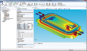
Figure 7 The picture shows the electric potential on the surface of a planar transformer.
CST
There is not, and never will be, a single tool that can do everything. Everything in the engineer’s toolbox – whether it is a physical item or a computer program – represents years of research and development into solving just a subset of the tasks that come up over the course of the design cycle. CAD and EDA tools make it possible to create complex designs rapidly, simulation tools allow engineers to model and optimize the system, and CNC machinery and test equipment can then be used to construct and analyze prototypes. Each one covers a part of design cycle, but for a complete integrated workflow, there needs to be interoperability between all of these tools.
CST STUDIO SUITE® is a simulation tool that includes numerous electromagnetic solvers, which help engineers model, simulate and optimize their designs. Because of the range of different design workflows that require simulation, straightforward interoperability with a wide variety of tools is of CST’s main goals when developing CST STUDIO SUITE, CAD and layout tools.
There are many CAD and EDA tools on the market, often focusing on different specific markets. The files these produce come in a wide variety of formats, with differing standards for model quality and shape representation. CST STUDIO SUITE includes import and export tools for general formats such as STEP, ODB++and GDSII, and proprietary formats from leading design and layout tools from vendors including Dassault Systèmes, Siemens, Mentor Graphics and Zuken.
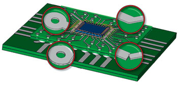
Figure 8 An imported model of a package, showing the automatic cleaning of faceted edges and healing of shape errors.
Automatic model cleaning and healing tools built into CST STUDIO SUITE make it easier to prepare CAD data for simulation purposes (see Figure 8), and imported models can be modified and parameterized just like native data. Even within a single team, there may be different departments working on different parts of the same product simultaneously since the engineers designing the logic board of an electronic device will not be the same ones who design the casing. The 2014 version of CST STUDIO SUITE introduced CAD data version control to make it easier for engineers in large teams to keep track of the work being done across different departments. CST STUDIO SUITE monitors the imported data and, if a file changes the user is notified. The model can then be automatically updated, with the changes highlighted and the model settings retained. Selective updating is also available for EDA files, in order to preserve the component, net and stackup definitions from the simulation model.
Once the model has been created, it needs to be simulated. CST STUDIO SUITE contains both full-wave 3D solvers and circuit simulation tools, along with specialized solvers for PCBs, cables and multiphysics applications. These solvers each have their own strengths, and can complement each other in many design workflows. CST’s Complete Technology approach to simulation means that these solvers are developed to work together. Not only does this allow a simulation to be cross-verified with a different solver, interoperability also unlocks the ability to combine simulation techniques and take advantage of the benefits of each.
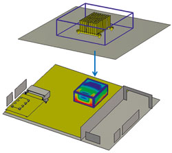
Figure 9 A nearfield source representing a heatsink in an EMC simulation of a router.
One common design project that benefits from this approach is emissions analysis (see Figure 9). An accurate calculation of the radiated emissions from a component usually requires a dense mesh around the component to capture its geometric details, but only a coarse mesh across the rest of the volume. Modeling the aggressor as a field source means that the most efficient mesh and simulation method for each part can be used. The same approach is also useful for problems such as antenna placement.
For a complex system, this approach may result in numerous different simulation and optimization tasks, all dependent on one another. For these, CST developed System Assembly and Modeling (SAM). With SAM, tasks such as simulation runs, parameter sweeps and post-processing can all be linked together and run as a chain. Different components can be linked together in the schematic view, and the transfer of signals, S-parameters and fields from one to another is handled automatically. CST STUDIO SUITE 2014 automates the process further, with tools to automatically set-up the SAM workflows for field-coupling and multiphysics workflows.
Many projects, especially in the world of EMC and compliance, straddle the border between virtual and physical testing. The engineer may have access to a prototype of a component, but not to the system it will be installed in, or the device may be designed to operate in an environment where measurements are difficult – whether that’s the depths of space or the human body. As well as offering advantages in virtual prototyping, interoperability with test equipment allows simulation to bridge the gap when measurement is impossible.
Measured data can be imported into CST STUDIO SUITE projects in a number of different ways. Both farfield and nearfield data can be used as the excitation for a full-wave simulation through the link to INSIGHT from Microwave Vision Group (see Figure 10), and measured S-parameters and I/O buffer information for components can be imported in formats such as TOUCHSTONE and IBIS. True transient/circuit co-simulation allows these elements to be directly included in a full-wave 3D simulation, even if they are nonlinear, and SAM can make the integration of measurement and both circuit-level and full 3D simulation straightforward.
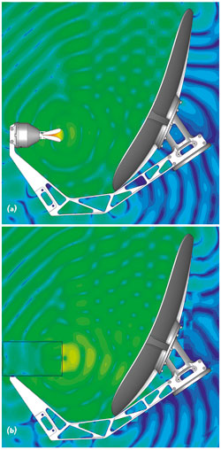
Figure 10 Simulation of a reflector antenna with (a) a 3D model of the feed horn and (b) an equivalent nearfield source created with INSIGHT.
CST also invests in developing links to third-party analysis tools, to help engineers make the most of simulation and tailor their results to the task. Among the compatible tools are Antenna Magus, for antenna and array design; Optenni Lab, for matching circuit optimization; Delcross Savant, for antenna placement, and Delcross EMIT for co-site interference analysis.
Delcross
About a year and a half ago, CST and Delcross cooperated to provide a workflow to take a complete CST analysis scene that incorporated several antennas, and import them directly into the Delcross EMIT software for RF cosite EMI analysis and mitigation. The idea is to make it easy for a CST user to take the EM results that characterized the complete antenna-to-antenna coupling in a given scene, pull it into EMIT and add system models for the transceivers, receivers, transmitters, amplifiers and outboard components (filters, cables), and look at the complete spectrum to search out in-band interference margin issues, broadband noise margin violations, and other issues that might lead to receiver desensitization.
In a specific example, a smartphone handset including multi-band cellular antennas, Wi-Fi, Bluetooth, NFC and navigation systems such as GPS and GLONASS was created in CST STUDIO SUITE. The model includes the antennas for the three systems of interest, and farfield monitors at key operating frequencies of the different systems. A simulation was carried out using the time domain solver across the spectrum from 0 to 6 GHz. This simulation provides both the S-parameters, which illustrates the wideband coupling (isolation) between each antenna, and the farfield patterns, giving the pattern degradation caused by installing the antennas in the environment of the handset.
Once all of the results have been calculated, the S-parameters, the field patterns and the CAD data can be transferred to EMIT in a single directory. After importing the files, the next stage is to define the RF systems themselves. EMIT includes a library of radios, power amplifiers, filters and other components, which can be assembled to produce a complete system. These models can include data such as channels, modulation and mixer products, as well as the programming of the radio.
With the RF systems defined, the potential for interference between the systems can be calculated. EMIT helps engineers investigating cosite interference consider the 1-on-1 scenario, where one system interferes directly with another, and the N-on-1 scenario, where multiple systems are transmitting simultaneously causing potential intermodulation problems.
Sonnet
In late 2013 Sonnet Software introduced an easy-to-use EDA environment for the analysis of on chip passive devices such as spiral inductors and MIM capacitors called BlinkTM. This multi-solver passive device modeling suite operates entirely from within the Cadence Virtuoso environment and offers users two full-wave electromagnetic (EM) solvers: Sonnet’s traditional shielded method-of-moments (MoM) solver, and a new fast solver that uses advanced algorithms to accelerate the device modeling process. Both solvers operate with PDK-specific stack ups, which can be customized for the user’s implementation.
Blink allows high frequency silicon circuit designers to include their stack up and PDK information in EM analysis with just a few button clicks. With Blink, integrated circuit designers now have an automated way to access electromagnetic analysis of passive RFIC devices without limiting them to any specific PDK. The new product automates the process of setting up electromagnetic simulations of passive integrated circuit devices including center-tapped spiral inductors.
Integrated circuit designers can now easily model new and unique passive devices within your normal Cadence Virtuoso based IC design flow. Blink’s new fast solver enables you to quickly characterize spiral inductors, baluns, transformers, MIM Caps, interdigitated capacitors, and transmission lines for radio frequency integrated circuit and mixed signal IC design.
