An integrated passive device (IPD) technology has been developed in order to achieve lower cost, miniaturization and higher performance in RF and microwave devices applied to the front-end modules of wireless communication systems. Various kinds of high performance IPDs have been fabricated on a six inch GaAs wafer due to the well-developed, low cost RF passive manufacturing technology. Since this article is primarily about the practical design and fabrication of IPDs, it will discuss topics such as IPD fabrication technology, design flow, schematic circuit design and 3D EM simulation. Different kinds of IPDs such as baluns, power dividers, lowpass filters (LPF), and their measurement results are presented.
In the electrical device industry, there is a trend for the integration and miniaturization of electronic systems, while steadily increasing performance, reliability and yield and reducing cost. Owing to the fact that IPDs are generally fabricated using standard wafer fabrication technologies, such as thin film and photolithography processing, they can be manufactured with these advantages and widely used in front-end RF sections of the mobile phone, comparable to embedded passive devices in an organic substrate or in low temperature co-fired ceramic (LTCC) substrates.1
IPDs, which contain passive circuit components such as resistors, inductors and capacitors, are totally integrated and mounted on a semiconducting substrate.2-4 Through IPD technology, it is possible to integrate individual passive components into an RF device or system.5 IPDs can be applied to existing fields of applications, which use whole passive devices and have already been applied to the front-end modules of mobile systems. In mobile phone communication systems, many functional blocks, such as filters, baluns/transformers, diplexers, power combiners/dividers, and couplers can be realized by IPD technology.6-10 In addition, the application of IPD technology to semiconductor processing is fully compatible with existing active devices and, thereby ensures semiconductor processing compatibility.
IPD Design Flow
There is a certain design flow that has been developed in order to simplify the design of IPDs. Specific design flows may vary among designers but, in general, almost all design flows are similar. In order to meet performance and cost targets, a general design methodology should be followed. This consists of the following steps: Choose the optimum topology and the right components from the design cell library that match the selected technology, and then perform the design by using software, such as ADS or AWR for a circuit-level simulation and a physical layout that fits the available space. After the layout, an EM simulation employing software, such as CST, is performed in order to optimize the component interaction, the wire-bonding with the pads and the packaging. In the next step, the various devices are arrayed and the masks are made for aligning the patterning. The designed devices are then fabricated using the semiconductor manufacturing process. The fabricated wafer is then thinned, using a polishing process, sawn using an automatic dicing saw, and assembled by die-bonding, wire-bonding and the SOT packaging process. Finally, the IPDs are subjected to the measurement of their DC, RF and power performances.

Fig. 1 Cross-sectional view of the GaAs IPDs.
Advanced Fabrication Process of Integrated Passive Devices
High-quality GaAs substrates and passive integration technology, characterized by accurate NiCr thin film resistors (TFR), high Q-factor spiral inductors and high-yield metal-insulator-metal (MIM) capacitors, enable the realization of fully integrated passive functional blocks. The proposed process starts with a first passivation layer, which is composed of SiNx and is deposited by plasma-enhanced chemical vapor deposition (PECVD) up to a thickness of 2,000 Å. This layer is necessary to attain an even surface over the defects and roughness of the substrate surface. After SiNx deposition, an e-beam-evaporated NiCr layer is deposited from a target consisting of 90 percent Ni and 10 percent Cr, in order to get the optimal performance. A Ti/Au 200 Å/800 Å layer, sputtered prior to plating process, is then used in order to increase the metal adhesion to the substrate. In the next step, the wafer is masked by photo-resist to define the structures of the bottom metal layer. Then, a 4.5/0.5 µm-thick Cu/Au metal layer is formed by electroplating, which is used as the contact metal for the NiCr resistors, bottom metal layer for MIM capacitors, and metal feedline and coils for spiral inductors. Now the MIM capacitor middle dielectric part has to be realized, a SiNx layer, 2,000 Å thick is deposited by PECVD and masked to define the structure. After the deposition step, a reactive-ion etching (RIE) step in O2/SF6 is performed to remove the undesired layer of the SiNx. Next, a 1,000 Å-thick Ti/Au seed metal layer followed by an air-bridge post-photo process is deposited by sputtering. Then, an air-bridge photo process is performed prior to a Cu/Au (4.5 µm/0.5 µm) top metal definition and plating process, by which top metal and air-bridge are made for the capacitor, and air-bridge interconnections are formed at the coil paths around the metal feedline for the inductor. After the electroplating process, the air-bridge mask is stripped, and RIE of the Ti/Au seed metal is done. Finally, all components are passivated with a thickness of 0.3 µm SiNx to protect the components from oxidation and moisture. The cross-sectional view of the GaAs IPDs is depicted in Figure 1.
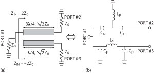
Fig. 2 Balun design using a transmission line (a) or lumped LCs (b).
Lumped L-C balun for WLAN Application
A balun provides balanced outputs from an unbalanced input. It is an important component in double-balanced mixers, push-pull amplifiers and the matching network placed between an antenna and the RF front-end system. Balanced output signals are defined as two output signals that have half of the input signal amplitude and are 180° out of phase.11-12 Generally, the easiest way to obtain a phase difference is by controlling the length of the transmission line. However, it requires a large length (λ/2) to achieve a phase difference of 180° at 2.4 GHz. An artificial transmission line can be used to provide a 180° phase shift in a small size by using lumped inductors and capacitors.13 This technique is used to convert the transmission line into lumped element circuits. A balun can be made using the relationship between the transmission line and the lumped element models, as seen in Figure 2. A compact 2.4 GHz wireless local area network (WLAN) balun designed and fabricated with a phase imbalance of less than 3° and very low insertion loss and high return loss is presented here.
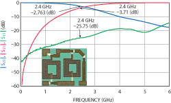
Fig. 3 Measured S-parameters for the fabricated WLAN balun.
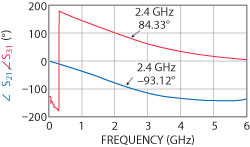
Fig. 4 Measured phase performance of the fabricated WLAN balun.
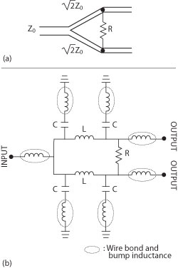
Fig. 5 Schematics of a typical power divider (a) and the designed DCS power divider (b).
After completing the layout, the circuit was fabricated using the GaAs IPD process created by NanoENS Co. Ltd. The fabricated chip was attached to the printed circuit board (PCB) using silver epoxy and bonded with gold wire. Measurements were then performed using a network analyzer over a frequency range of 100 MHz to 6 GHz. The insertion loss of the designed balun is affected by the core inductances of Lp and Ls; the design width of the core inductors is 15 µm. The balun was fabricated with a die size of 800 × 700 × 200 µm. Its RF performances are shown in Figures 3 and 4; the insertion loss and the return loss were below 0.25 dB and 25.75 dB, respectively. The phase imbalance was less than 3° and its amplitude imbalance was less than 0.5 dB.
Lumped L-C Type Power Divider for DCS Application
Power dividers are frequently used in transmitter and receiver systems, providing equal power division with an in-phase response. The power divider splits the input power into two or more output ports; it is a potentially lossless device, provided that no power is reflected from its output ports. Power dividers need to be matched at all ports; the output ports need to be isolated.14-15 A typical two-way power divider includes an isolation resistor (R = 2Z0) and two λ/4 transmission lines with an impedance of Z0, where Z0 is the characteristic impedance of the power divider. The schematic diagram of a typical two-way power divider is shown in Figure 5. The power divider circuit can be converted, as seen in the figure, by using the relationship between the transmission lines and the lumped element models. The inductance effects of the interconnections between the output ports and ground also need to be taken into account. For the bond-wire and bump inductance, the required inductance values are 0.36 and 0.02 nH, respectively. To be able to achieve low losses and a wide bandwidth, inductors with relatively high resonant frequencies and large Q-factors are required. A small 1.8 GHz digital cellular system (DCS) power divider with a very low insertion loss, a high return loss and good isolation was designed and fabricated.
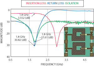
Fig. 6 Measured insertion loss, return loss and isolation for the fabricated DCS divider.
After completing the layout, the circuit was fabricated using the GaAs IPD process. The final required R, L, and C values were determined after optimization. The fabricated DCS power divider, with a die size of 850 × 750 × 200 µm, and its RF performances are shown in Figure 6; the insertion loss is below 0.56 dB, the return loss is below 30 dB, and the isolation is better than 27.5 dB around the center frequency. The amplitude imbalance between the output ports is approximately 0.1 dB; the phase difference is 1° at the operating frequency.
Lumped L-C Type Lowpass Filter for WLAN Application
LPFs are an essential component in many electrical circuits for passing wanted signals and to eliminate or attenuate harmonics. The filter design starts from the synthesis of a standard third-order Butterworth LPF using lump elements.16 A shunt capacitor Cs is added to the inductor Ls in order to create a transmission zero at approximately 5.6 GHz. Since there is only one spiral inductor in this filter design, only one capacitor can be added to create one resonant transmission zero. The inductance is also adjusted to achieve a good input-matching in the passband. The schematic circuit and 3D structure of the designed LPF are given in Figure 7.
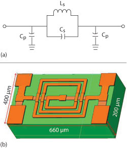
Fig. 7 Schematic of the designed WLAN LPF (a) and the CST simulation structure (b).
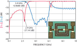
Fig. 8 Measured S-parameters for the fabricated WLAN LPF.
There are many differences found between the circuit level simulation and the EM simulation results. In order to minimize this gap, a circuit-tuning method using the internal ports is used in this LPF design.17 By using this optimization method, a response closer to the specifications was achieved. Figure 8 shows a photograph of the 2.4 GHz WLAN LPF with a die size of 660 × 400 × 200 µm. The insertion loss was typically 0.56 dB at 2.4 to 2.5 GHz, and the return loss was below 27 dB. The attenuation level in the second-harmonic frequency was less than -25 dBc.
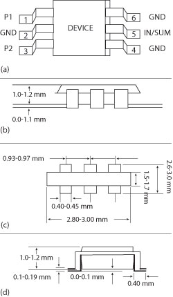
Fig. 9 The SOT package schematic for the fabricated IPDs (a) full view, (b) side view, (c) top view and (d) front view.
SOT Packaging and Power handling Measurement
The use of semiconductor wafers is a cost-effective way to simultaneously fabricate many chips. Once all of the fabrication and testing is complete, the chips are separated from the wafer and assembled into the final integrated circuit (IC) package. The assembly and packaging process takes the approved electrical devices, places them in a package and interconnects the device bonding pads to the package leads. The packaging provides a means of protecting the chip from the environment and from handling damage, provides physical support for the chip heat dissipation, interconnection for the signals in and out of the chip, and for attaching it to a high assembly level.18 In this work, SOT packages were used for the fabricated IPDs, which are small in size and allow a higher board density, leading to a higher electrical speed for system applications. The SOT packages are of the cheap surface-mount plastic-molded type, with leads on their two longer sides in order to achieve a low cost and a low profile. The SOT package schematics are illustrated in Figure 9.
In general, power dividers and LPFs are usually located next to the power amplifier in order to split the power or remove the harmonic signals. Therefore, the power handling capacity is a very important factor in power dividers and LPFs. How to measure the power handling of the fabricated power dividers on the GaAs substrate will be shown as an example. Figure 10 shows the system used for the power divider’s power handling measurement. The incident power of the power divider can be measured by using a {20 dB coupler and the output power of the power divider by using a {40 dB attenuator and a spectrum analyzer. For the first test, 3.5 W of RF continuous wave power is injected into the input of the power divider. After 10 hours of operating time, the incident power is increased in 2 W steps. Due to its good thermal conductivity, the power divider on the GaAs substrate endured up to 12 W of incident power during the 60 hours step test. Figure 11 shows the measurement results of the power divider after the 12 W power handling tests.
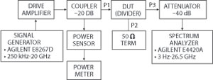
Fig. 10 Measurement system for the power handling evaluation.
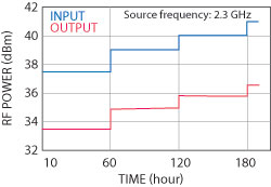
Fig. 11 Power handling measurement results.
Discussion
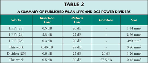
The IPDs measurement data are compared with other literature for similar devices using the same frequencies. The IPDs fabricated in this work show the lowest insertion loss and the best return loss characteristics with the smallest die size. This data shows the best results for the designed IPDs compared to the other IPDs. Tables 1 and 2 show the WLAN balun, LPF and DCS power divider that were fabricated by NanoENS Co. Ltd.’s manufacturing process compared to other previously produced devices.

Conclusion
Compact-size RF IPDs were successfully fabricated on GaAs substrates with high power handling capability and low loss. The WLAN balun with a die size of 800 × 700 × 200 µm was fabricated, which showed an insertion loss of 0.25 dB and a return loss of 25.75 dB. The phase imbalance was measured to be less than 3°; the amplitude imbalance was less than 0.5 dB. The power divider for DCS application shows insertion loss of 0.56 dB, return loss of 30 dB, and isolation of 27.5 dB with a die size of 850 × 750 × 200 µm. An LPF is also fabricated for 2.4 GHz WLAN applications and has an insertion loss of 0.56 dB, a return loss of 27 dB and attenuation level at the second-harmonic frequency less than -25 dBc. The “cheap and compact” IPDs are achieved by using passive integration technology on GaAs substrates and SOT packaging method, while maintaining their high power handling capability and RF performances. Such IPDs are suitable for use in various handheld modules and system applications that require an effective cost, stringent size and high performance.
Acknowledgment
This research was supported by the National Research Foundation of Korea (NRF) grant funded by the Korean government (MEST) (No. 2011-0030819). This work was also supported by the Research Grant of Kwangwoon University in 2012.
References
- R. Ulrich and L. Schaper, Integrated Passive Component Technology, IEEE Press/Wiley, New York, NY, 2003.
- K. Zoschke, J. Wolf, M. Topper, O. Ehrmann, T. Fritzsch, K. Scherpinski, H. Reichl and F.J. Schmuckle, “Fabrication of Application Specific Integrated Passive Devices Using Wafer Level Packaging Technologies,” IEEE Transactions on Advanced Packaging, Vol. 30, No. 3, August 2007, pp. 359-368.
- C. Wang and N.Y. Kim, “Fabrication of Metal-Insulator-Metal Capacitors with SiNx Thin Films Deposited by Plasma-Enhanced Chemical Vapor Deposition,” Transactions on Electrical and Electronic Materials, Vol. 10, No. 5, October 2009, pp. 147-151.
- C. Wang, F. Zhang and N.Y. Kim “Development and Characterization of Metal-insulator-metal Capacitors with SiNx Thin Films by Plasma-enhanced Chemical Vapor Deposition,” Chinese Physics Letters, Vol. 27, No. 7, July 2010, pp. 078101_1-078101_4.
- H.M. Clearfield, J.L. Young, S.D. Wijeyesekera and E.A. Logan, “Wafer-level Chip Scale Packaging: Benefits for Integrated Passive Devices,” IEEE Transactions on Advanced Packaging, Vol. 23, No. 2, May 2000, pp. 247-251.
- L.J. Liu, S.M. Kuo, J. Abrokwah, M. Ray and D. Maurer et al, “Compact Harmonic Filter Design and Fabrication Using IPD Technology” IEEE Transactions on Components and Packaging Technologies, Vol. 30, No. 4, December 2007, pp. 556-562.
- K. Liu, R. Emigh and R.C. Frye, “Small Form-Factor Integrated Balun with Complex Impedance Matching,” 2008 IEEE MTT-S International Microwave Symposium Digest, pp. 1239-1242.
- D.W. Kim, I.H. Jeong and J.S. Lee, “Passive Miniaturization: Si Integrated Passive Devices for RF and Microwave Applications,” Microwave Journal, Vol. 45, No. 11, November 2002, pp. 78-88.
- C. Wang, J.H. Lee and N.Y. Kim “High-performance Integrated Passive Technology by Advanced SI-GaAs-Based Fabrication for RF and Microwave Applications,” Microwave and Optical Technology Letters, Vol. 52, No. 3, March 2010, pp. 618-623.
- J.W. Jung, K.K. Nae, J. Kim and J.S. Park, “RF-IPD Directional Coupler for Mobile RFID Handset Applications,” Electronics Letters, Vol. 43, No. 13, June 2007, pp. 719-720.
- C.H. Tseng and Y.C. Hsiao, “A New Broadband Marchand Balun Using Slot-Coupled Microstrip Lines,” IEEE Microwave and Wireless Components Letters, Vol. 20, No. 3, March 2010, pp. 157-159.
- Y.K. Jung and B. Lee, “Design of Compact and Wideband Metamaterial Balun Based on Closed-form Solutions,” Microwave and Optical Technology Letters, Vol. 52, No. 5, May 2010, pp. 1153-1156.
- S.J. Parisi, “180° Lumped Element Hybrid,” 1989 IEEE MTT-S International Microwave Symposium Digest, pp. 1243-1246.
- Q. Li, X.W. Shi, F. Wei and J.G. Gong, “A Novel Planar 180° Out-of-Phase Power Divider for UWB Application,” Journal of Electromagnetic Waves and Applications, Vol. 25, No. 1, January 2011, pp. 161-167.
- S.W.Y. Mung and W.S. Chan, “Compact Tunable Lumped-Element Wilkinson Power Divider with High Isolation,” Microwave and Optical Technology Letters, Vol. 53, No. 2, February 2011, pp. 288-290.
- S.A. Mahmoud, “Low Power Low-Pass Filter with Programmable Cutoff Frequency Based on a Tunable Unity Gain Frequency Operational Amplifier,” Journal of Circuits, Systems and Computers, Vol. 19, No. 8, December 2010, pp. 1651-1663.
- R.B. Ekinge, “A New Method of Synthesizing Matched Broad-Band TEM-Mode Three-Ports,” IEEE Transactions on Microwave Theory and Techniques, Vol. 19, No. 1, January 1971, pp. 81-88.
- Y. Liu, L.H. Liang, S. Irving and T. Luk, “3D Modeling of Electromigration Combined with Thermal-Mechanical Effect for IC Device and Package,” Microelectronics Reliability, Vol. 48, No. 6, June 2008, pp. 811-824.
- I.H. Jeong, J.Y. Kim, B.J. Lee, J.J. Choi and Y.S. Kwon, “Comparison of RF Integrated Passive Devices on Smart Silicon and Glass Substrate” Microwave and Optical Technology Letters, Vol. 45, No. 5, June 2005, pp. 441-444.
- I.N. Jeong, K.J. Kim, T.O. Kong, J.S. Kim and H.K. Choi et al, “High Performance RF Integrated Passive Devices on Thick Oxide Substrate Using Cu-BCB Process” Microwave and Optical Technology Letters, Vol. 37, No. 1, April 2003, pp. 49-52.
- C.H. Huang, T.C. Wei, T.S. Horng, S.M. Wu and C.C. Wang et al, “High-Performance Marchand-type Balun Design and Fabrication Using an Integrated Passive Device (IPD) Technology,” 2008 International Conference on Electronic Materials and Packaging Digest, Taipei, China, pp. 137-140.
- J.C. Park and J.Y. Park, “Lattice-type Balun with Enhanced Phase Characteristic Based on Organic System on a Package Technology,” Microwave and Optical Technology Letters, Vol. 51, No. 2, February 2008, pp. 399-402.
- C.M. Nam and I.H. Jung, “High Performance RF Integrated Circuits Using the Silicon Based RF Integrated Passive Device (RFIPD),” 2005 International Conference on Information Communications and Signal Processing Digest, Bangkok, Thailand, pp. 1357-1361.
- K. Zoschke, J. Wolf, M. Topper, O. Ehrmann and T. Fritzsch et al, “Thin Film Integration of Passives – Single Components, Filters, Integrated Passive Devices,” 2004 Electronic Components and Technology Conference, Las Vegas, NV, pp. 294-301.
- J.P. Yang and W. Wu, “Compact Elliptic-function Low-pass Filter Using Defected Ground Structure,” IEEE Microwave Wireless Component Letters, Vol. 18, No. 9, September 2008, pp. 578-580.
- I.H. Jeong, C.M. Nam, C.Y. Lee, J.H. Moon and J.S. Lee et al, “High Quality RF Passive Integration Using 35 µm Thick Oxide Manufacturing Technology,” 2002 Electronic Components and Technology Conference Digest, San Diego, CA, pp. 1007-1011.
