

NOTE: When working on things like papers and simulations, there is not much need for time-domain analysis. However, the methods discussed in this article can be leveraged on practical engineering situations for a variety of useful functions, including:
Simulation Model Debugging:
From a time-domain simulation model, you can generate an averaged-state AC model to evaluate loop responses and the methods reliably identify potential errors between those models.
Pulse Loading Applications:
You can test high-power pulse-operating RF by using a VRM, but first you may need to confirm that your VRM offers DC bias sourcing impedance low enough for your RF circuits. The downside is that the VRM can overheat in continuous wave (CW) conditions when running a frequency-domain analysis.
High Voltage Applications:
When designing 48 V power bus applications, you may need to test your 48 V output VRM BUT could have difficulty measuring such a high voltage node into 50 Ω-terminated frequency-domain analyzers (VNAs: vector network analyzers, or FRAs: frequency response analyzers).
For each of these examples, methods in this article provide a potential solution. A best practice is to start with known data or known behavior to compare with. The goal of this post is to give you more tools to evaluate output impedance ZOUT.
Our goal is to execute the following steps.
STEP-1: Take a time-domain measurement on our voltage regulator module (VRM)
STEP-2: Monitor the time-domain response of our VRM
STEP-3: Derive the frequency-domain characteristic ZOUT of our VRM
Again, Figure 8 from part 8 provides a simplified block diagram of our VRM target. This diagram assumes that our VRM consists of an ideal DC power source VVRM and an output impedance ZO.

Figure 1. Sub-simulation treatment of the VRM model
In Step-1, we apply a time-domain changing signal at the VOUT node. Because we have the VVRM pure DC source inside our VRM, it is not practical to drive the VOUT node by another voltage source, as unlimited current may flow into or out from the VRM. So, we drive our VRM by a current source. This is what power electronics engineers call a "load transient" test.
Next, we must decide on the type of load transient signal we want to use. Many control loop theory textbooks start by using a unit impulse signal δ(t) or an impulse response test to probe frequency-domain characteristics / parameters from the time-domain.

Let’s see what happens to our VRM if we apply an impulse load current.
 Figure 2. Impulse Load Transient ⇐ Precision data processing needed!
By connecting an ideal impulse current source IIMPULSE to the VRM, this impulse current makes a voltage drop across ZO, and we observe the output voltage for Step-2:

By comparing our impulse load transient test setup and a textbook impulse response test as listed below, we can see that our monitored voltage signal follows the textbook impulse response techniques. So, we can reconstruct our VRM output impedance from the load transient response.
Textbook approach to Impulse Response Test
- A test for a transfer function of amplifiers or filters.
- The target transfer function takes voltage signal input and outputs voltage signal output.
- The resulting output voltage signal expression is a product of the transfer function and input voltage signal.
This article: Impulse Load Transient Test of Output Impedance
- A test of output impedance.
- The output impedance allows current input signal through the element and generates a voltage drop signal.
- The resulting output voltage signal expression is a product of the impedance and input current signal.
Scientifically, the impulse signal is a generalized function; in other words, it is a super-natural, unrealistic signal. When we take this path, we need precise data sampling and processing. This series introduces power integrity in practical ways. So, we will use an alternative signal for our load transient test.
As many readers might expect, we will use a unit step function u(t), instead of an impulse signal δ(t). In both simulations and bench tests, we can generate our unit step u(t) signal to the level where we can ignore its non-ideal errors by making the step slew rate as fast as possible.

With the applied load step, our expected observed output voltage signal is now:


Figure 3. Step Load Transient
Textbooks, teaching us the benefits of impulse response tests, also explain the relationship between the impulse signal δ(t) and a step signal u(t) as shown in Figure 4.

Figure 4. Impulse δ(t) and Step u(t)
From Figure 4, a mathematical derivation d/dt of the step response Eq. 10-4 is identical to an impulse response:


Per Eq. 10-6, we can get our VRM output impedance by manipulating our observed step-response voltage waveform with a sequential derivative followed by Laplace-transform processing.
Simulations
By running QSPICE™ simulations, we confirm that this concept is working. All the simulation slide decks are available at the Qorvo repository on GitHub. There, the PyQSPICE module, written in Python, handles all the data arrangements, calculations and plotting, and those operations are recorded using a Jupyter Lab.
1st Simulation, Confirmation of Concept
We start our simulation with a simple circuit with a known result. This first simulation session file is here.
Our first simulation is a textbook LCR parallel resonant circuit with a Quality factor Q = 10 and a resonant frequency at 159.2 kHz.
In the schematic, the gray box is a step event generator with a simulation time-step control, which is a QSPICE “.DLL” (dynamic link library) written in C++. This block places more simulation time steps around the step event in order to produce finer resolution results.

Figure 5. First Simulation Schematic, Q=10 Resonant
By running an AC simulation, we can see that it has its resonant frequency at 159.2 KHz with Q = 10. Please refer to Eq. 9-5 in part 9 for the Q(Tg) function definition..

Figure 6. First Simulation: AC Simulation Result, Q=10 Resonant
In the next step, we run a load transient simulation with a unit step current source. This simulation runs for a total 10 ms period, and we have only one step (low to high) event at 5 ms, which is the center of the total simulation period. The 10 ms period of the simulation waveform means our frequency resolution is down to 100 Hz (= 1 / 10 ms). Our step transient in 1 ns contains enough high frequency energy to the sub-GHz range, which is more than enough to confirm our 159.2 kHz resonant behavior.

Figure 7. First Simulation: TRAN Simulation Result, Q=10 Resonant
Now, we run our data manipulations and compare the AC simulation result and  Please note that, in this data processing, we use Fast Fourier-Transform (FFT) because the Fourier-Transform and the Laplace-Transform act in the same way for one-shot event waveforms (not continuous signal).
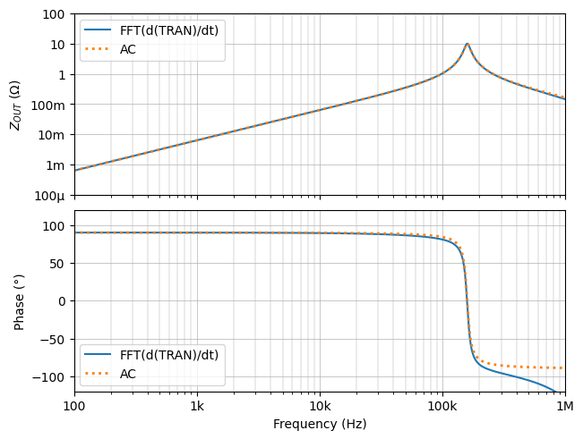
Figure 8. First Simulation: Proof of Concept, Q=10 Resonant
From this plot, we can assert that this concept of determining output impedance from the step load transient is valid.
For readers to review the step-by-step operation of this result, please check the session file.
Please note that to obtain these well matching curves, we use 32k data points (data lines) for our complex-number (gain and phase) data operations. From a practical engineering perspective, this quick method of obtaining reliable results is a valid and useful tool.
Second Simulation, Model of VRM Output Impedance
In our second simulation, we use an ideal model of VRM output impedance. This second simulation session file is here.
Our second simulation schematic is modeling the output impedance of a VRM.
- The left box represents a VRM with 5V output and 10mΩ impedance at low frequency, with 100 nH inductance that will lead to higher impedance as frequency increases.
- The middle block represents an output capacitor of 1 μF, 1 mΩ ESR, and 1 nH parasitic inductance, which results in a 5 MHz self-resonant frequency.
- We have a dummy load of 500 mΩ.

Figure 9. Second Simulation: Schematic, VRM Output Impedance Model
By running an AC simulation, we can see that this model represents the VRM of loop BW ~500 kHz and Q ~ 1.5. Because of the “Cout” and “Lesl” pair, we have a sharp anti-resonant peak at 5 MHz but this is a result of output capacitor modeling.

Figure 10. Second Simulation: AC Simulation Result, VRM Output Impedance Model
In the next step, we run a load transient simulation with a unit-step current source. This setup is the same as the first simulation.

Figure 11. Second Simulation: TRAN Simulation Result, VRM Output Impedance Model
Now, we run our data computations and compare the AC simulation result and just like the first simulation.

Figure 12. Second Simulation: Proof of Concept, VRM Output Impedance Model
Because we need to reconstruct the curves close to 10 MHz for our simulation period of 10 ms, we use a million data points. By looking at the compared curves, we can confirm that this method is applicable beyond 10 MHz assuming we have a large data set. With the power of the gray C++ control block, we can achieve this high accuracy to the high frequency region. For readers to review the step-by-step operation of this result, please check the session file.
With the speed of the QSPICE and Python programs, we can get this plot in a couple of minutes.