

Overview
The output impedance characteristic of VRMs (Voltage Regulator Modules), ZOUT, plays a big role in our power integrity discussion, probably the leading player.
Just as RF or signal-chain engineers care about impedance and matching, power engineers care about VRM and power distribution network (PDN) impedance, to optimize power integrity performance.
Why is output impedance so important?
- In almost all cases, we can access and measure a VRM’s ZOUT curve on the test bench. All we need is to probe a PCB trace with our test equipment to measure a ZOUT curve in a largely non-invasive manner, where there is no need to remove components or to cut PCB traces.
- A VRM’s ZOUT is the starting point for PDN impedance analysis of any power rail.
- The last and the most important factor: a VRM’s output impedance ZOUT is a direct measure of its control loop performance.
Every probe measurement is invasive to some extent, altering the original DUT (Device Under Test) behavior, but a VRM feeds DC voltage to its load devices from low impedance and with high power driving capabilities. An additional parallel 50 Ω probe will have negligible effect unless dealing with low-power LDOs or switching regulators for mobile/portable applications.
Textbooks, for example [1], teach us that closed-loop output impedance ZOUT(Closed) is a function of the VRM loop transfer function T(s) and open-loop output impedance ZOUT(Open) (Eq.8-1)
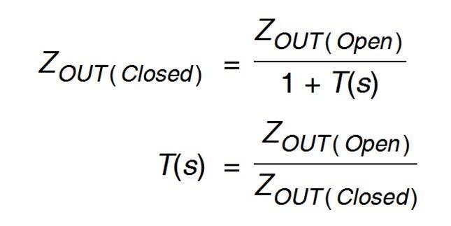 Eq. 8-1
By running various example simulations in QSPICE™, we review the relationship between output impedance characteristics, ZOUT, and the control loop for a VRM.
Simulation model
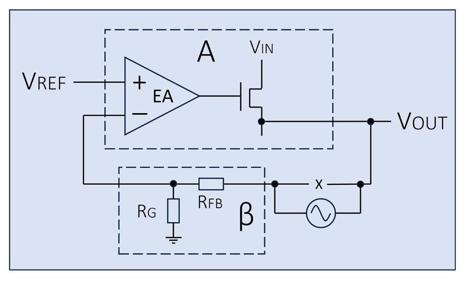
For our review of a VRM’s output impedance ZOUT, we’ll reuse a previous linear-regulator simulation model example with some additional elements. As we proceed, we will see the reasons for these extra circuit blocks.
This simulation deck is available at Qorvo repository at GitHub.
 Figure 1: Linear regulator simulation analyzed for loop response
This simulation deck runs 6-steps of sub-simulations, with the ‘.step’ (dot step) statement.
| Bode Plot | Zout(Closed) | Zout(Open) |
Error Amp, Loop #0 | Step = 0 | Step = 2 | Step = 4 |
Error Amp, Loop #1 | Step = 1 | Step = 3 | Step = 5 |
Notes:
- Two different gain profiles are in the error amplifier block, and we will compare the difference in the review process. This difference comes from the gain stage of pair R1 and Cea in the schematic and the two profiles alternate in the odd and even number of steps.
- The voltage source Vac provides perturbations for the Bode plot.
This source is ON at steps 0 and 1 and OFF afterwards. - The current source Izout provides perturbations for the output impedance curves. This source is OFF at steps 0 and 1, and ON for steps 2-5.
- By changing the cut-off frequency of the L2/C1 filter pair, we make an open loop simulation for ZOUT curves. With this LC filter, we can maintain its very low-frequency DC bias point, i.e. the output voltage Vout stays at its target value when the loop is opened. This filter is OFF at steps 0-3 and ON at step 4 and 5.
Though we will review each result in detail in the following sections, the results of all six steps are shown in Figure 2.
 Figure 2: Phase and gain responses from simulation
+/ – signs and 180° shift
If you want to copy details of the simulation circuit, calculations and plots in this post, this section provides information about how voltage potential polarity and current flow direction are set.
Loop transfer function, opening the loop and the Nyquist diagram
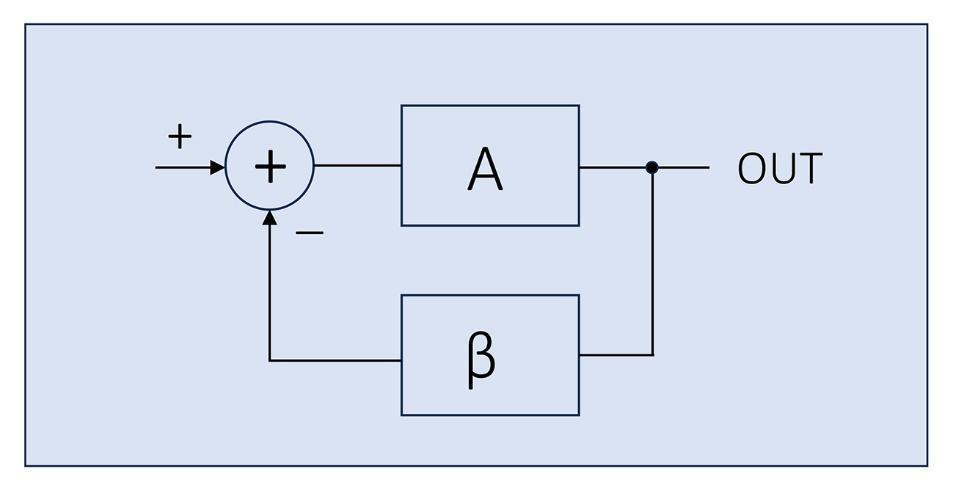
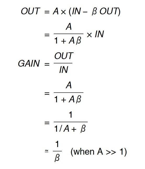
In the textbook, it explains the basics of a negative feedback loop in Figure 3 with the characteristic equations shown in Eq.8-2
Eq. 8-2
When discussing the Nyquist stability criterion and Nyquist diagram, we deal with a loop transfer function T = Aβ that is available by opening/cutting the loop at ‘X’ as in Figure 4.

Figure 4: The basic feedback loop opened
Note that we cut the loop at the summing point of the ‘+’ and ‘–’ signals, which means there’s no negative summation in this loop-opening method.
We can re-draw our simulation circuit to match Figure 3 as shown in Figure 5.
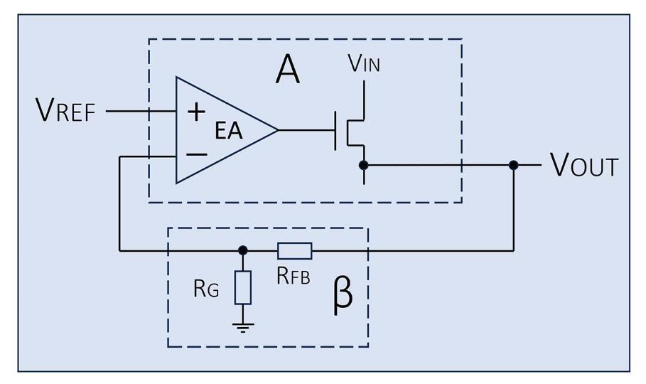
Note that the error amplifier in the original schematic is driving a P-type FET gate and the feedback signal is connected to the ‘+’ port but acting as a negative ‘–’ port.
For our ‘.STEP’ = 0 and 1 of the Bode plot sub-simulations, we insert our AC perturbations by opening the loop as shown in Figure 6. Note that by opening the loop in this way, we have executed a ‘negative summation’ so the resulting loop transfer function is shifted 180°.
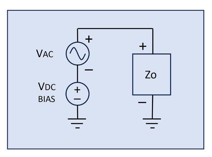
Output Impedance
When measuring an impedance, use the circuit of Figure 7, where a sinusoidal ‘positive peak’ supply causes a ‘positive peak’ on the target component being measured. This could be done either by:
- Applying AC voltage and measuring AC current flow into the target
- Applying AC current and measuring AC voltage across the target
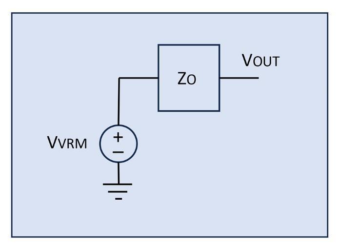
For our ‘.STEP’= 2 - 5 of the impedance sub-simulations, we treat the VRM model as in Figure 8.
We apply our AC perturbations and monitor the Vout signal which represents the output impedance (Figure 9).
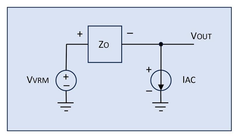
Note that assuming a VRM core block can be represented by an ideal DC voltage source, this measurement setup sends a positive peak current source to measure a negative peak of voltage response, so the resulting signal Vout is a 180° shifted version of our output impedance.
Reconstructing the loop transfer function from ZOUT
Now, it’s time to execute the calculation by following equation Eq.8-1, reconstruct the loop transfer function by paying attention that these simulation results are phasor signals, in another words, vector data holding phase as well as amplitude information.
The pair of gain and phase plots in Figure 10 are the loop #0 on the left side and the loop #1 on the right side.
Because this is a set of ideal simulations, we can see our reconstructed loop transfer functions from ZOUT(Closed) and ZOUT(Open) are perfectly matching the original Bode plots. Knowing this is too good to be true, visit the Qorvo repository at github.com for the entire simulation kit, to double-check these exact matching curves by running your own simulation runs.
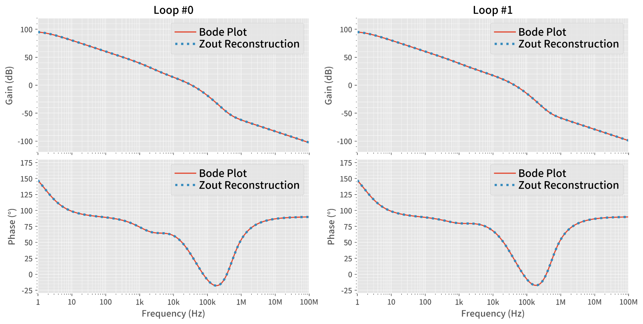 Figure 10: Gain and phase plots from simulation
For confirmation, the same data is re-plotted in a different grouping: the Bode plot simulation on the left side and the reconstructed loop transfer function from ZOUT(Closed) and ZOUT(Open) on the right side. Here, we can see the differences between the two loop profiles of #0 and #1, clearly shown on both sides, especially in the phase plots.
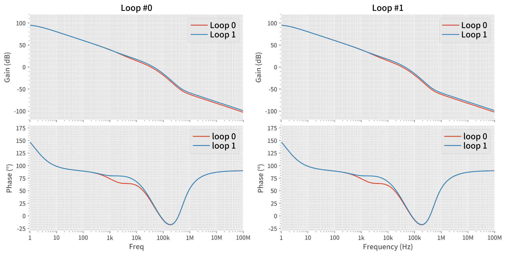 Figure 11: Gain and phase re-plotted
Remember that both the simulations for the Bode plots and the reconstruction from ZOUT are 180° shifted compared with generic control loop theory textbooks.
In our plots, we can see around 30° of phase margin when the gain crosses the 0 dB line. This is a result of our simulation setup with results shifted by 180° such that 0° margin leads to oscillation. It is a little odd to say "we have around 150° degree margin from the 180° point", but it’s the same thing as flipping the ‘ +’ and ‘–’ signs.
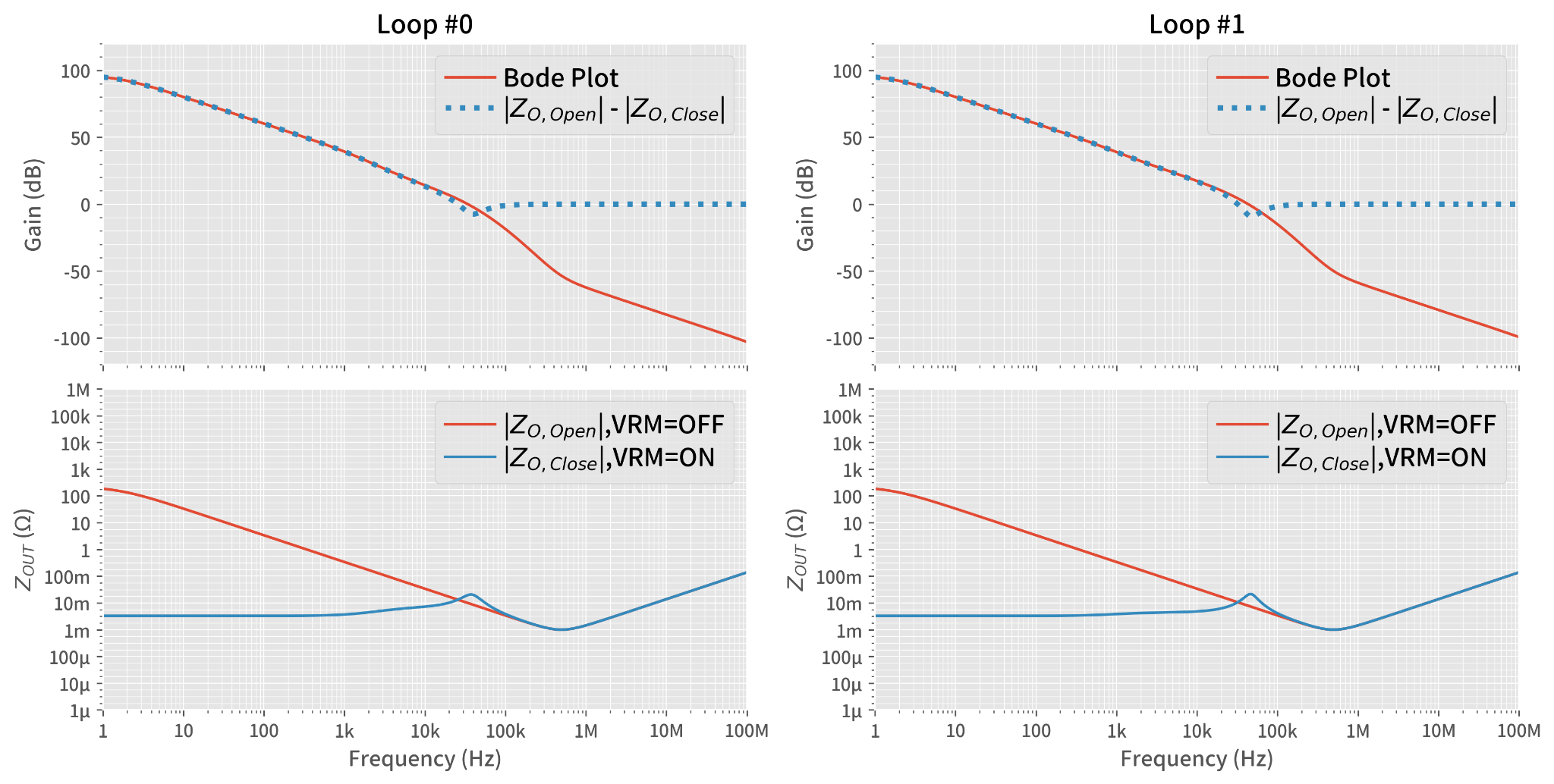
Looking at equation Eq.8-1, we can ignore the ‘– 1 ’ 2nd term when the first term ZOUT(Open) / ZOUT(Closed) is big enough, meaning just use the 1st term ZOUT(Open) / ZOUT(Closed) to represent the loop transfer function down to around unity gain, 0 dB. Furthermore, when we plot the impedance on a logarithmic scale, this ‘open’ to ‘closed’ ratio turns into a delta. So, we can do a quick check of our loop transfer function without vector / phasor calculations and all that is needed is simple math: ZOUT(Open) (dB) – ZOUT(Closed) (dB)
Figure 12 is the plot of this quick-check version of the reconstructed loop transfer function, shown in the blue dotted line. As explained, this plot is good down to 0 dB but worth knowing, as we can outline the loop transfer function without any calculation tool as you measure the ZOUT plot. Note that we can also access the phase information with this quick subtraction version.
[1] Fundamentals of Power Electronics, 2nd Edition (Robert Erickson and Dragan Maksimovic, Springer Science+Business, 2001)