
This paper describes a concept of non-adaptive Digital Feed-forward Linearization. A feed-forward amplifier is a system designed to reduce the spectrum re-grows appearing due to the amplifier’s nonlinearity.
There are several general techniques to reduce nonlinearity effects. They are divided into two major groups. One of them (called “predistortion”) is geared toward preventing nonlinear effects from appearing. According to this technique, the input signal is distorted in a specific way allowing an output signal to be distortion-free. The second group (called Feed-forward Linearization) focuses on compensation of those effects after their appearance. In that technique the input signal remains unchanged. All the corrections are done to the output signal by adding correcting waveforms in anti-phase to distortions.
Each of the groups has its advantages and disadvantages. Predistortion is cheaper and less cumbersome, but has its physical limitations of the degree of compensation.1 Feed-forward Linearization has no limitations of compensation in principle, but is more difficult to implement. The implementation of Feed-forward Linearization can be done by either analog or digital means. In analog implementation, distortions are extracted from the output signal (by comparing distorted with undistorted signals) and then added in anti-phase to the output. In digital implementation, the distortions are generated by software means and then, as in the case of analog, are added in anti-phase to the output. The main advantage of digital implementation is in the accuracy of created signals. There is no need to extract distortions from the output signal. Since their nature is known, they are created precisely. The need for adaptation (real-time adjustments based on the degree of distortions) is reduced or eliminated entirely.
In this paper the theory of a spectrum re-growth creation is introduced. Based on it, the scheme for corrections is developed. The traditional analog method of Feed-forward Linearization is given and the advantages of a digital method are shown. One of these advantages is in the knowledge of the nature of sidelobes, which makes it possible to use a non-adaptive compensation. Simulations and experiments are shown to confirm this concept.
Basic Theory
Any nonlinear system can be described by the equation:
eout=k1ein+k2ein2+k3ein3+... (1)
where ein is an input signal, eout is an output signal and ki are complex coefficients.
Modern wireless communications deploy digital data streams as input signals. Their spectrum is represented by the function of the type of [sin (x)/(x)].2 Due to the nature of this function, higher order components spread the spectrum. Additional spreading is happening because of Root Raised Cosine filtering. Only the odd components of Equation 1 add to that spectrum spread.3 In wireless communications, harmonics are filtered out. The output signal of the nonlinear system for wireless communications is represented by Equation 2:
eout=k1ein+k3ein3+k5ein5+... (2)
A typical graphical presentation of a data stream spectrum, its cube and its fifth power is shown in Figure 1.

Figure 1 Spectrum of a typical data stream (main), its third order and its fifth order.
The combination of these waveforms creates the resulting signal according to Equation 2. The reason for sidelobes is the presence of higher order components. In order to eliminate a spectrum spread caused by nonlinearity, it is natural to create higher order waveforms and apply them in anti-phase to the output signal.
Analog Feed-Forward Linearization
Traditionally, the generation of correcting waveforms (that is, waveforms intended to get rid of nonlinear effects) was done by analog means. The reason for that was in the nature of input signals, which were analog. All the information about distortions was extracted from the output signal, amplified and then added in anti-phase to that same output signal (see Figure 2,4 where VM is a vector modulator, a device used for adjustments of amplitude and phase of the signal).
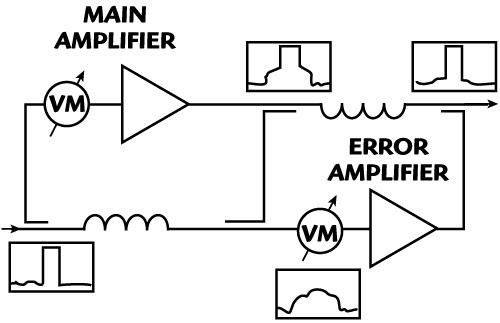
Figure 2 Traditional feed-forward linearization.
The problem with this approach is in accuracy of distortions’ extraction. Analog extraction is inaccurate in principle (since it depends on real-time conditions). In addition, RF components used for the extraction are not ideal, so they are enhancing the uncertainty of the extraction.
In the systems employing digital data streams as input signals, the accuracy of nonlinear compensation can be significantly increased with simultaneous reduction of the circuitry complexity. Creation of the correcting waveforms by digital means achieves this goal.
Digital Feed-Forward Linearization
Digital Feed-forward Linearization is also intended to correct unwanted nonlinear effects in power amplifiers at its output, only it does so by digital means. It works because of a digital nature of input signals. The waveforms in the systems employing digital data streams are created by means of software, that is in the DSP. In software, it is relatively easy to apply predetermined mathematical functions to those waveforms. Specific mathematical functions required for linearization are the odd powers of the initial signal (that is, its cube, fifth order, etc.). When these functions are applied, the results are to be multiplied to the corresponding coefficients (k3, k5, etc.) and added with the opposite sign to the output waveform represented by Equation 2. This will lead to a perfect correction of nonlinearity effects.
The signal given by Equation 2, however, is a RF signal (since it represents an output of RF power amplifier). To implement the compensation described above, the functions created in the DSP have to be converted to RF. The multiplication by the corresponding coefficients is also done in RF using vector modulators (similar to Figure 2). Vector modulators maintain the required phase and amplitude plus allow the application of adaptation techniques (if required).
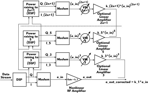
Figure 3 Digital feed-forward linearization.
The block diagram depicting this approach is given in Figure 3. This block diagram consists of a number of branches corresponding to the number of powers to which the initial signal is raised. As in every wireless application, the data stream is applied to the DSP, divided to I & Q, conditioned and applied to the modem where it is converted to RF. The unique feature of Digital Feed-forward Linearization is that I & Q are applied not only to the modem, but also used to create additional waveforms. At each of the additional branches, the I & Q are applied as input waveforms, converted to the complex form (with I as real and Q as imaginary), raised to the required power and divided again to their own I & Q conditioned data streams. The newly obtained I & Q are applied to the corresponding modems and the resulting RF signal is applied to the vector modulators for amplitude/phase adjustments. The outputs of vector modulators are amplified by linear amplifiers (if necessary; usually, the value of k3 is about 30 to 40 dB below the value of k1. This means that in the majority of practical realizations no additional linear amplifiers are needed. However, in the unusual case of a high-gain high-level-of-nonlinearity amplifier, the device similar to the “Error Amplifier” in Figure 2—marked as “Optional Linear Amplifier” on Figure 3—can be added to the system) and added in anti-phase to the output of the nonlinear RF amplifier.
In practical realization, no more than two additional branches are expected, since the influence of higher than fifth-order additions are small. However, as it will be shown later, up to four branches might be required.
It is good to note that in contrary to the previous Feed-forward Linearization schemes,5,6 the described approach does not necessarily need any adaptive methods. Digital Feed-forward Linearization does not change anything at the input signal; it creates additional signals. By its nature it does not require any adaptation techniques, since all the variations of the power amplifiers’ parameters (like frequency, power level and operational temperature) can be predicted and included into control circuitry of vector modulators. However, if prediction of those parameters for any reason is undesirable, adaptation feedback loops for controlling the vector modulators can be included.
ADS Software Simulations
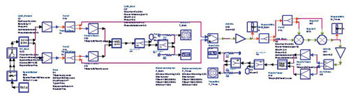
Figure 4 Creation of a cube signal from the main signal in a DSP.
The implementation of the creation of main and cube signals in the DSP (using ADS software from Agilent) is given in Figure 4.
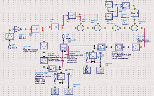
Figure 5 Block diagram of the amplifier's behavioral model.
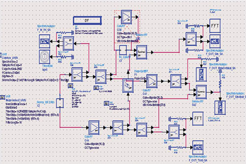
Figure 6 Block diagram of digital feed-forward linearization.
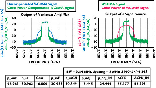
Figure 7 Results of simulations on the behavioral model.
The initial simulation, intended to understand the capabilities of the suggested linearization in principle, was conducted using a custom-made behavioral amplifier model. The main signal was applied to the input of the behavioral amplifier model (see Figure 5) and the cube branch was used for the compensation at the output of the model (see Figure 6). The results, obtained for the source of a WCDMA signal, demonstrating a perfect compensation, are given in Figure 7.
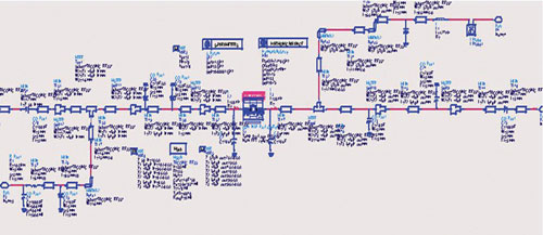
Figure 8 Matching structure for a 10 W GaN transistor model.
The reason for the perfect compensation is in the chosen composition of the behavioral model, which represents a creation of only up to the third power of distortions. While the model is fully expandable, it is more convincing to conduct simulations using a model of a real amplifier. For that purpose a model for a 10 W GaN amplifier from NXP Semiconductors was chosen and placed in a matching structure (see Figure 8).
The goal was to substitute the model in the matching structure for the nonlinear amplifier in the block diagram of Digital Feed-forward Linearization, as seen in Figure 6. In order to avoid a co-simulation between ADS’s RF and DSP benches, a block diagram similar to the one in Figure 6 (with a source similar to the one on Figure 4, only with five branches instead of two) was assembled in RF bench. In order to speed-up the computation process, instead of the model itself, large-signal S-parameters in p2d format were extracted from the model (see Figure 8) and used for the simulations. To avoid computation complexity, no feedback between output spectrum and correction signals was used, and a required ratio of amplitudes and phases for correction signals was determined manually.
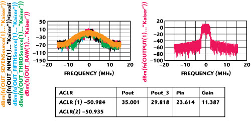
Figure 9 Results of simulations on a GaN amplifier model.
The results are shown in Figure 9. Due to the noisy nature of the waveform’s presentation in ADS’s RF Bench, the maximum achievable value of ACLR is 51 dBc. This level of compensation is reached with four additional branches of compensating signals (3rd, 5th, 7th and 9th order). When only three additional branches are used, the value of ACLR is 47 dBc, which is good enough for meeting WCDMA requirements. Two branches give the value of ACLR of only 41 dBc, which is also below the limit for the standard.
The given model for a GaN transistor was not checked for its linearity effects, so it is not clear how accurately it predicts the number of required branches for an ideal compensation. However, for the purpose of this paper it is not important. What is important is a demonstration that an ideal level of compensation can be achieved for any given amplifier while using a described approach.
Experimental Confirmation
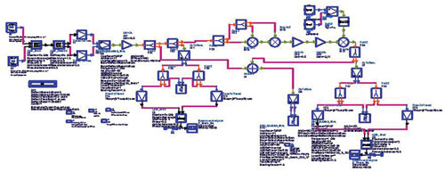
Figure 10 Block diagram for uploading main and cube signals into Agilent 4438B.
There is a method for a direct experimental confirmation of a Digital Feed-forward Linearization approach. Rohde & Schwartz offers a Vector Signal Generator (SMU200A), that has two independent RF outputs with synchronized basebands. However, as a substitute, another generator (Agilent 4438B) was employed to confirm the results. This generator has only one output, so the results had to be confirmed indirectly. The method of confirmation has the same idea of compensating waveforms created by digital means, only created waveforms where applied to the amplifier’s input (predistortion). For simplicity, only two branches (main and cube) were used in experiment. This method was simulated and the values of amplitude and phase for compensating the cube waveform were found. A block diagram for uploading the waveforms (with a signal source in OFDM format) from ADS to Agilent 4438B is shown in Figure 10.
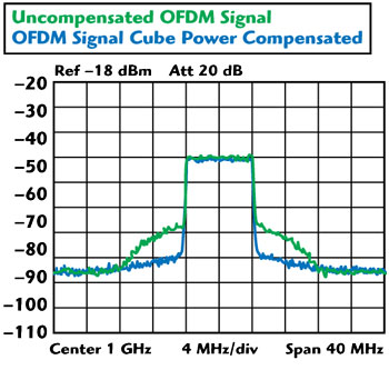
Figure 11 Experimental results.
A generator’s output was connected to the input of RFMD amplifier RF2314 and its output spectrum was monitored. Initially the generated cube waveform was attenuated (so only the main waveform appeared at the amplifier’s input), and a resulting spectrum was recorded. Then the amplitude and phase of the cube waveform were adjusted according to the predictions of ADS simulation. The sidelobes of the initial spectrum were eliminated, as seen in Figure 11.
Conclusion
In this paper a concept of non-adaptive Digital Feed-forward Linearization—an approach intended to correct unwanted nonlinear effects in power amplifiers—is described. It is based on the creation of additional compensating waveforms in the DSP and their conversions to RF. The explanation of the concept was given and supporting simulations were conducted. Experimental results made with simple arbitrary generated waveforms confirm predictions.
The implementation of this concept is relatively simple and all the RF hardware of a traditional feed-forward amplifier is reusable. The only requirement is access to the baseband of the base station, where the feed-forward amplifier is located. When access is gained, the correcting waveforms are generated from the baseband’s data stream, converted to RF and applied to the output of the main amplifier. It is expected that in the majority of cases no error amplifiers are going to be needed. The parts count of a feed-forward amplifier is reduced, which reduces the amplifier’s cost and improves its reliability.
The described approach to Digital Feed-forward Linearization does not require adaptation techniques. That is, no additional feedback circuitry is needed for the system to work in principle. However, introducing a feedback adaptation would help with keeping near perfect compensation over temperatures, frequencies and power levels.
References
1. B. Aleiner “The Concept of Predistortion,” Microwave Journal, Oct. 2003.
2. B. Aleiner “Comparing the Impact of PAR on ACP in Wireless Designs,” CommDesign, February 2002.
3. K.A. Simons “The Decibel Relationships Between Amplifier Distortion Products,” Proceedings of the IEEE, Vol. 58, No. 7, July 1970.
4. Y.Y. Woo, Y.G. Yang, J.H. Yi, J.G. Nam, J.H. Cha and B.M. Kim, “An Adaptive Feed-forward Amplifier for WCDMA Base Stations Using Imperfect Signal Cancellation,” Microwave Journal, April 2003.
5. J.H. Pan and A.J. Brammer, “Digital Feed-forward Active Noise Control System,” US Patent # US5852667.
6. D.U.L. Yu and P.H. Conway, “Feed-forward Digital Phase and Amplitude Correction System,” US Patent # US5365190.
Boris Aleiner earned his MSEE degrees from Leningrad Polytechnic University, St. Petersburg, Russia, and Drexel University, Philadelphia, PA. Over his career as a wireless RF engineer, he has been working for major telecommunication companies focusing on nonlinear amplifiers and methods of their linearization. He has published a number of papers and holds several US patents on the subject of RF wireless components/subsystems. Currently he is an independent consultant.