
In the fiercely competitive GSM phone terminal market, terminal manufacturers have come to expect solutions that expedite their development and cycle times. Coupled with the new feature-rich handsets with mega-pixel cameras, Bluetooth® technology and multimedia functions, designers are demanding smaller and more integrated modules that consume less board space while delivering superior performance levels. RF Micro Devices’ designers have developed the RF3177 and RF3178 transmit modules (TxM), aimed at meeting these market needs. A transmit module is comprised of a combination of power amplifier (PA), controller, harmonic filters and antenna switch — all in one module.
TxM Benefits Explored
Besides the obvious benefits of smaller size and reduced component placements, in what areas does a TxM offer advantages for designers over a more discrete implementation?
Lower Insertion Loss in Tx and Rx Paths
A TxM includes the antenna switch functionality by incorporating any number of switch configurations and internal architectures. Common module architectures include two Tx path switches, a 3- or 4-Rx path switch with a common node going to the antenna.
While early switch modules were predominately PIN diode-based, newer designs take advantage of a customized pHEMT switch design to achieve similar or better performance. Among others, a real benefit to pHEMT-based designs is the lower insertion loss through the switch.
With careful design techniques in both the pHEMT switch legs and the harmonic matching filters, the insertion loss on Tx signal paths can be minimized. By keeping the insertion loss as low as possible, the PA output power is transferred more efficiently to the antenna. This is possible to do in a TxM because designers have intimate knowledge of the PA output match combined with control over the match/filter and pHEMT input. That gives the designers a degree of flexibility difficult to find when mating current power amplifier module (PAM) and antenna switch module (ASM) solutions. This is possible because the TxM designer is no longer constrained to be in a 50 ? output environment. He can choose the appropriate impedance to match the amplifier output, typically 2 to 4 W, and match that to a pHEMT switch directly (see Figure 1).
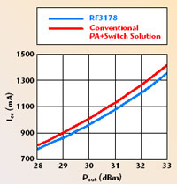
Fig. 1 1cc vs. Pout for the RF3178 at fTX=900 MHz.
The reduced insertion loss results from being able to eliminate the task of transforming to 50 W at the PA output and ASM input. This removes up to 0.5 dB of loss in the transmit chain, resulting in a net savings for the GSM mode of 150 mA and on the order of 90 mA for PCS/DCS.
Similarly, the receive (Rx) internal matching topology also benefits from the absence of a 50 ? transformation, therefore deriving the same benefit on the Rx side of the TxM. The resultant, lower Rx insertion loss (IL) translates into increased Rx sensitivity. Table 1 summarizes data for comparison of Rx IL using RF3178 and traditional dual- and tri-band ASMs; Figure 2 shows the Rx IL from antenna to the LNA input.

Fig. 2 Rx insertion loss from antenna to LNA input.
Improved Harmonic Performance
With the ever-increasing importance of time to market, design re-use is a common theme among developers, leading to an increasing number of phone platforms. The trend to this platform development approach is becoming more and more visible, whereby a radio transceiver and PA+ASM combination will be used across many handset designs. Many difficulties are encountered when this “known” platform is used in multiple form factors. Specifically, handset form factors such as clamshell, candy bar and sliders all present different antenna mismatches to the radio modem as well as variations in PCB properties. Thus a platform that works well in one form factor may perform much differently in another, typically to the detriment of overall performance. Antenna differences are usually the main culprit under those conditions.
Radio platform designers can benefit by having a tightly controlled PA output, harmonic filter and switch interface. TxM designers are presented with a controlled environment within a TxM, with which they can optimize (reduce) harmonics emanating from the PA. This piece of the radio design then becomes a true platform transferable to various form factors with the confidence that performance contained within the TxM is guaranteed through electrical specification from the manufacturer, something that cannot be said for typical platform PA+ASM section designs. Even after handset designers complete a robust design, any modifications to the delicate match can significantly alter the impedance and affect the harmonic levels measured at the antenna. By maintaining the integrity of that interface, TxM designers have a much better chance of suppressing harmonics under extreme conditions, even under mismatch conditions. For example, it is typical for TxM designs to achieve harmonic levels less than –30 dBm into a 4:1 VSWR over all extremes, as shown in Figure 3. That makes for a very robust solution capable of use under many form factor design considerations.
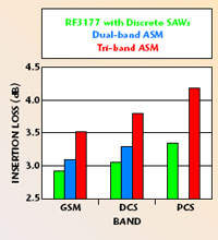
Fig. 3 Typical harmonic levels at 900 MHz into a 4:1 VSWR with Pout at 33 dBm.
Flexible Transceiver Signal Routing
As mentioned, the latest TxMs utilize pHEMT switches in the design. The advantage of using a pHEMT switch for the antenna switch portion is that the Rx ports can be configured in just about any manner that the routing requires. The pHEMT input frequency response is broadband, allowing virtually any port to be designated as either high band or low band (see Figure 4). This enables a single GSM TxM to be used independent of any specific transceiver. This should be especially useful in ODM environments, where it is common to be sourcing two to three different transceiver configurations, predominately based on baseband choices, but with a design to maintain a single PA sourcing strategy with key high volume suppliers.
Fig. 4 Rx path frequency response showing band pass filter characteristic.
Potential for WCDMA Antenna Pass-through
One especially convenient area for emerging multimode applications is the ability to designate one of the unused ports as a pass-through port for a separate WCDMA Tx/Rx signal. During this transition time toward multimode there is often a need for quick, bolt-together solutions utilizing separate WCDMA and GSM/GPRS radio chains. The ability to utilize an unused port in a GSM/GPRS TxM for switching eliminates the need for a separate ASM and supporting matching components for the WCDMA radio chain, enabling both cost and size savings. RFMD has tested and characterized the pHEMT switch ports for linearity and intermodulation at WCDMA frequencies and power levels. The results show it is feasible to use one of the Rx ports for a WCDMA pass-through.
Other Considerations
One of the “ease of use” features found in most commercially available TxMs is an integrated ESD protection at the antenna port. This consists of an on-board inductor-capacitor circuit to suppress any high voltage short duration impulse from damaging modem components. This is particularly useful because most SAW filters on the Rx path are very susceptible to ESD transients. Additionally, these ESD filters comply with the 8 kV contact discharge requirements of IEC 61000-4-2.
As part of an ongoing trend, newer generations of integrated modules are continually challenged to reduce the amount of external components required to implement radio solutions. The same applies with TxMs. In fact, TxMs specifically target these integration needs as a fundamental premise of existence. Not only is the number of external components reduced, the need for delicate, intra-component matching circuits are also eliminated. With TxMs, designers enjoy an overall size reduction in the layout area required for similar functional implementation. Typical figures show anywhere from a 30 to 50 percent layout area reduction versus comparable PA+ASM solutions (see Figure 5).
Fig. 5 Typical PCB layout using PA and ASM.
Reduced Phone Platform Development Time
As demonstrated, the TxM is a very robust solution due directly from the use of on-board matching circuits that are optimized for key areas such as power flatness, harmonics and performance into a VSWR. Its true benefit is in lower development cost. A TxM solution that meets desired performance over a VSWR will greatly reduce development time and consequently shorten time to market. Implementing a TxM in an application is a matter of verifying performance instead of designing and fine tuning delicate RF circuitry, which is the common procedure with traditional PA+ASM solutions. The reduction in phone platform development time can have a significant impact on a handset’s ability to come to market faster. Time to market (TTM) has been touted as a top metric of handset manufacturers as they vie for position in the handset space.
A Truly “Tamper-proof” Solution
Countless stories abound from situations where once stable reference designs had to be adjusted in the field, sometimes extensively, because a handset manufacturer had chosen to use a different PA+ASM combination than what was originally intended. The manufacturer’s reasons are usually sound ones — the other component may offer some price savings that are attractive, delivery issues, etc. The downside is that more engineering effort needs to be called in to repair a system that was already approved for FTA. Supporting these many manufacturing variants can be daunting and expensive, and can represent significant hidden costs for both reference design providers as well as PA suppliers. Hence, more profits can be retained by deploying a tamper-proof solution and TxMs are newly emerging as a key component in achieving this.
Conclusion
In understanding all the benefits contained within, TxMs are expected to represent an important part of the company’s 2005 shipments with a significant increase in demand occurring through 2006. RF Micro Devices® has made its presence known in this market with the first generation of TxM, RF3177, aimed at the quad-band GSM/GPRS market. Subsequent to this product, the RF3178 is a key component in the POLARIS™ 2 TOTAL RADIO™ Module offering for EDGE handsets. Combined with size reduction and an increase in overall performance, the RF3178 is designed to support polar modulation in combination with the POLARIS 2 Radio Module solution. Additional TxM products aimed at both polar modulation and GSM/GPRS markets are planned for 2005.
RF Micro Devices Inc.,
Greensboro, NC
(336) 678-5570,
www.rfmd.com