
Microstrip resonators have very important applications in microwave or millimeter-wave systems. They are important components of microstrip filters, microstrip oscillators and microstrip antennas, and enable miniaturization of microwave equipment with improved performance. The performance of a microstrip resonator relies on the electromagnetic field distribution, the resonant frequency and the quality factor, Q. Microwave high-Q resonators are traditionally made of metallic rectangular or cylindrical waveguides, which are heavy, costly to manufacture and difficult to integrate with monolithic circuits.
Microwave and millimeter-wave planar integrated circuits having low loss and high-Q are gaining popularity and demand. Compared to standard topologies, they offer cost-reduction, planarity and improved performance, and can be fabricated easily on silicon substrates due to micro-machining capabilities. They are also amenable for integration into a compact, stable package meeting environmental requirements.
Resonators, using bulk micro-machining on high resistivity silicon substrates with interface layers of oxide and nitride, have been described by Papaloymerou, et al.1 But the effect of a low resistivity wafer on the performance was not discussed. It was stated by some authors that the effect of substrate resistivity becomes negligible when using interface layers of oxide and nitride. This article demonstrates the considerable effect of the substrate resistivity on the performance of the micro-machined resonators, in spite of using passivation layers. Two similar microstrip lines resonators, with one fabricated on a high resistivity silicon (HRS) substrate (ρ > 7 kΩ-cm) and the other on a low resistivity CMOS grade silicon (LRS) substrate (ρ ≈ 3 to 5 Ω-cm), have been compared. For accurate measurement of the quality factor, the structures were made lossy by using a weak coupling, using displacement of the slots rather than narrowing down the slot dimensions.2 The use of polyimide has found great potential due to its compatibility with the MMIC and CMOS integration processes, leading towards an RFIC/SoC concept. This article details the configuration, fabrication steps and a comparison of the measured results of all the fabricated topologies.
Resonator Analysiss
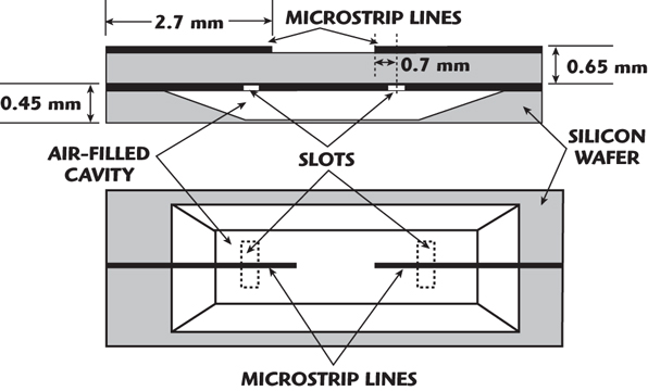
A planar micro-machined resonator is shown in Figure 1. Two stacked wafers, the bottom one including a micro-machined cavity, are eutectically bonded. The top wafer couples the electromagnetic energy into the cavity through the two slots and acts as a feed. By using the equivalence principle, the slots can be replaced by perfect electric conductors with equivalent magnetic currents flowing above their surface. Thus, the cavity and the microstrip lines are separated by the ground plane of the microstrip lines. The lumped equivalent model of the resonator is also shown in Figure 2.
The slots are modeled by ideal transformers and the cavity behavior by an RLC parallel circuit. The altering of the slot positions is equivalent to changing the transformer turns ratio, which in turn changes the response bandwidth. The magnetic coupling is ensured by two microstrip lines through the two slots located in the ground plane of the top wafer. These two apertures provide magnetic coupling to the cavity. The coupling coefficient between the microstrip lines and the cavity can also be controlled by the size and location of the slots. By decreasing the slot distance, the bandwidth can be reduced.3 The design of the micro-machined cavity resonators is based on the theory of rectangular cavities. The resonators are operated in the fundamental TE101 mode. The resonant frequency of the cavity is evaluated using the following equations:

where l, w, h are the cavity length, width and height, and m, n, o are the Eigenvalues 1,0,1 for the fundamental mode. The microstrip width and height is denoted as W and h.
Fabrication
The X-band resonator is fabricated using standard micro-machining techniques.4 Two silicon wafers, 675 μm thick, are stacked together with the bottom wafer micro-machined to realize the cavity using a KOH etch. Two variants are fabricated, one having a high resistivity top wafer and a low resistivity wafer at the bottom (HRS). The second has low resistivity wafers at both top and bottom (LRS). The microstrip lines, made of Cr/Au, were fabricated using E-beam metallization and patterned by a lift-off lithography technique. The bottom of the feed (top wafer), which contains the coupling slots, was aligned and metallized (Cr/Au) by a lift-off process and acts as a ground plane. Oxide (0.5 μm) and nitride (0.25 μm) layers were deposited on the low resistivity wafers using a LPCVD process.
To make the cavity, the low resistivity silicon bottom wafer is etched with KOH to a depth of 0.45 mm by controlling the etch rate. The bottom wafer is then metallized with 1 μm gold. The top and bottom wafers are stacked together using eutectic bonding. The wafers are misaligned during bonding so that after dicing the wafer a small opening is created, which acts as a ground and facilitates testing in the microstrip mode itself. The length and width of the cavity are selected to be 15.5 and 15.38 mm, respectively, to get a resonant frequency of approximately 12.5 GHz. The slots are placed nearer to the open-ended feed line rather than a &lamda;/4 distance away to introduce a weak coupling and consequently increasing the losses. This results in an insertion loss of approximately 10 dB, thereby facilitating the accurate measurement of the quality factor. The slot width and length are kept approximately 0.63 and 2.9 mm, respectively.
The cavity is then filled with polyimide after the normal fabrication steps. The polyimide is cured for one hour at 120°C and sealed with a conductive epoxy. The total assembly is further cured for one hour.
Results and Discussions
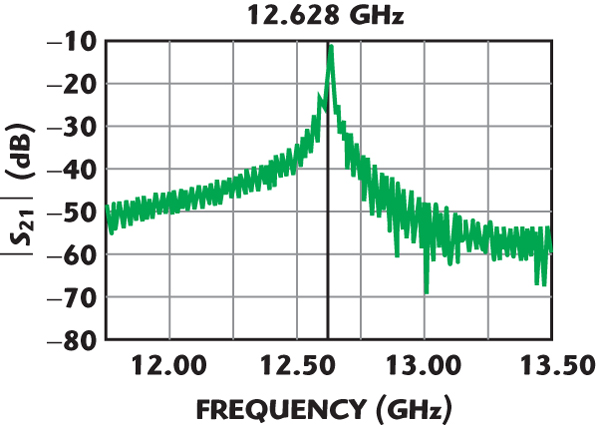
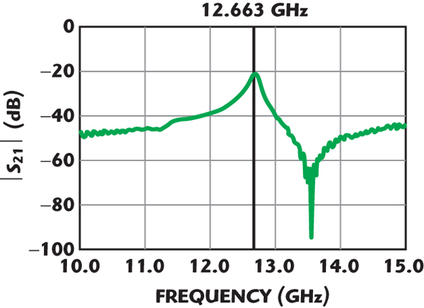
A simulation study was carried out on the two resonators using the 3D simulator from CST5 based on the finite element method (FEM). The simulated results of the two kinds of resonators are shown in Figures 3 and 4, respectively. It can be seen that the simulated resonance is approximately 12.5 GHz, but with a difference of 10 dB in the insertion loss. The measured results are shown in Figures 5 and 6, respectively. The results show an insertion loss of approximately 12 dB for HRS and 21.5 dB for LRS at approximately 11.5 GHz.
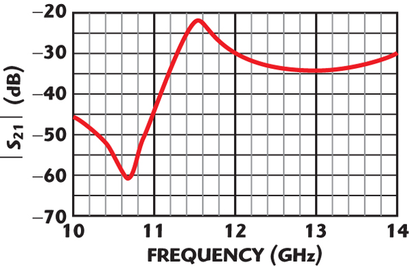
The measured difference of 9.5 dB in insertion loss is in close agreement with the simulated 10 dB difference. The increase in insertion loss of approximately 2.0 dB is attributed to the conductor loss and other parasitics introduced in the testing. The conductor loss can be overcome by increasing the metallization thickness.
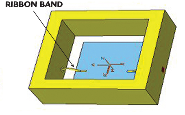
The measured results show a resonance frequency lower by 1.5 GHz from the simulated value. This can be explained as follows: the structures are tested in the microstrip mode by introducing a ribbon bond. A 20-mil ribbon with a 2 mm length introduces an inductance of approximately 0.32 nH, resulting in a lower frequency. The simulations carried out to validate this drift used the jig shown in Figure 7.
The singly loaded Q of the structures can be calculated as8

The value achieved shows a much higher Q than the microstrip structure. The eutectic bond strength is measured using a bond pull/die shear tester (DAGE-22 A) on a number of structures and a minimum bond strength of 5 g is observed.
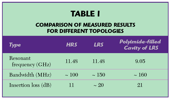
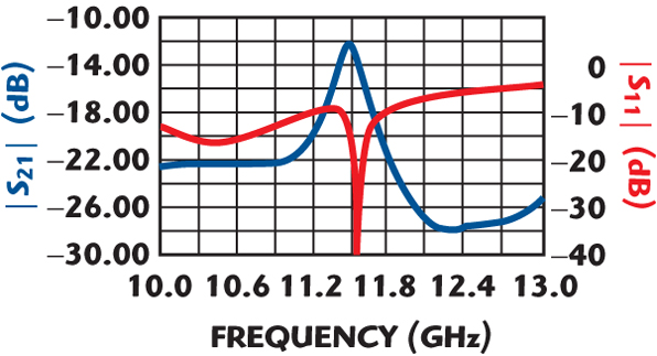
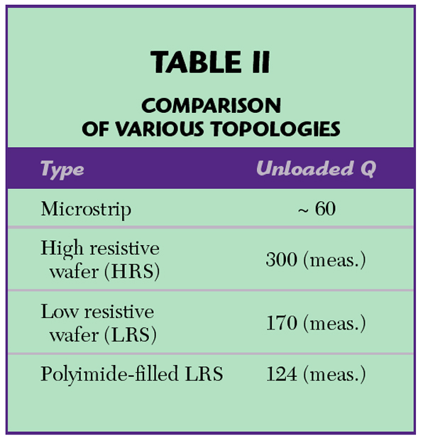
The polyimide-filled cavity changes the effective permittivity, resulting in a value close to 1.625. This results in a resonant frequency theoretically close to 9.05 GHz, which is also validated by practical measurements. The frequency scaling has been done without compromising the size of the structure. Tables 1 and 2 compare the results of all the topologies previously discussed.
Conclusion
The effect of substrate resistivity and polyimide filling on the RF performance of micro-machined resonators has been detailed in this article. The resonators realized using low and high resistivity substrates showed a difference of 10 dB in insertion loss as expected. Also, the different structures give identical resonant frequencies in spite of passivation layers of oxide and nitride in case of the LRS structure.
The polyimide-filled cavity lowers the resonant frequency by 2.5 GHz. This shows that frequency scaling can be done without increasing the size of the structure. This property can be useful for designing low frequency circuits without increasing the size. Also, due to polyimide compatibility with the MMIC/CMOS processes, the structure finds a wide range of applications.
The structures also show repeatable performances. The quality factor achieved in these structures is much higher than that achievable with a microstrip configuration. The measured Q is less than the simulated one due to extra parasitics involved while testing. Considering all these aspects, including the size reduction and the measured bond strength, these structures are suitable candidates for the development of narrow band filters in the planar environment.
References
1. J. Papaloymerou, J.C. Cheng, J. East and L.P.B. Katehi, “A Micro-machined High-Q X-band Resonator,” IEEE Microwave and Guided Wave Letters, Vol. 7, No. 6, June 1997, pp. 168–170.
2. Hill, J. Papaloymerou and Zilokowski, “High-Q Micro-machined Resonant Cavities in a K-band Configuration,” IEEE Proceedings on Microwave Antenna and Propagation, October 2001, pp. 307–312.
3. L. Harle, J. Papaloymerou, J. East and L.P.B. Katehi, “The Effects of Slot Positioning on the Bandwidth of a Micro-machined Resonator,” European Microwave Conference Digest, 1998.
4. M. Stickel, G.V. Eleftheriades and P. Kremer, “High-Q Bulk Micro-machined Silicon Cavity Resonator at Ka-band,” Electronics Letters, Vol. 37, No. 7, March 2001, pp. 433–435.
5. CST Microwave Studio, 2006 B.
6. G. Duchamp, L. Casadebaig, S. Gauffre and J. Pistre, “A New Tool for Slot-microstrip Transition Simulation,” IEEE Microwave and Guided Wave Letters, Vol. 7, No. 9, September 1997, pp. 276–278.
7. C. Schollhorn, M. Morschbach and E. Kasper, “Attenuation Mechanism of Aluminum Millimetric-wave Coplanar Waveguides on Silicon,” IEEE Transactions on Electron Devices, Vol. 50, No. 3, March 2003, pp. 740–746.
8. R. Rhea, “EM Enables Classic Filter Technique,” Microwave Journal, Vol. 50, No. 2, February 2007, pp. 138–146.
Kamaljeet Singh received his MS degree from Rajastan University and his M. Tech (microwaves) degree from Delhi University in 1999. He joined the ISRO satellite center, Bangalore, in 1999, where he worked in the receiver division. Since August 2006, he has been working in the RF MEMS area of the Semiconductor Laboratory, Chandigarh, India.
K. Nagachenchaiah received his BE degree in electronics and communication engineering and his M. Tech degree in computation and control engineering from Andhra University and IIT Kharagpur, respectively. He joined the Space Applications Center, Ahmerabad, in 1974, and was involved in the design and development of various optical infrared remote sensors for aircraft and space platforms, ground-based instruments and sensor test facilities. He is currently the director of the Semiconductor Laboratory, Chandigarh, India.