
One of the major applications for ferrite junction components is in base station amplifiers. Each amplifier module may include several isolators, which typically provide mismatch protection. In the case of the isolator placed between the power amplifier and the antenna, the primary purpose is protection against high levels of reflected power. The form factor of these isolators is a drop-in, in which the large termination chips attached to the isolator base plate are capable of absorbing up to 200 W average power. Situated after the power amplifier, the isolator must handle the full RF power of about 100 W or more. Since each base station amplifier may have several channels, nonlinear distortion will present a problem. Various linearization methods are used to limit distortion in the amplifier, but they do not help reduce distortion in the isolator (except perhaps crest factor reduction). The ferrite materials used in isolators are fairly linear up to a few watts. Above this level, the most significant nonlinear effect is third-order intermodulation distortion (IMD). This is the result of two (or more) signals of different frequencies (F1 and F2) interacting in a region with nonlinear transmission properties.1 The third-order distortion products that may interfere in the receiver pass band are the difference frequencies 2F1–F2 and 2F2–F1. Higher order distortion products are usually several decibels lower in amplitude. If third-order products are reduced, the higher order products should also drop by a similar amount. IMD is measured as the ratio in power levels between the distortion signal and the input signal, in units of dBc. Typical IMD levels for isolators are approximately –80 dBc for two signal tones of 20 W each. Usually ferrite isolators obey the theoretical behavior for varying the input signals, that is, for each 1 dB change of input level, the IMD level changes by 2 dBc.
ANALYSIS
The generation and behavior of distortion signals can be worked out mathematically by assuming that a nonlinear medium causes an output, which can be expressed as a power series
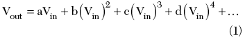
where a, b, c and d are constants, Vin is the input voltage, which in the case of two input frequencies is equal to V1 cos (ω1t) + V2 cos (ω2t). The phase can be ignored for this purpose, and inserting this expression for Vin into Equation 1 yields
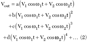
When the individual terms are multiplied out, the third-order output is given by
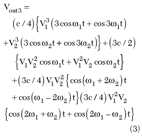
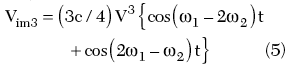
Collecting only the difference terms for the third-order intermodulation distortion yields
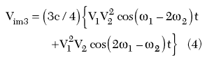
When the input signals have the same amplitude V
Since the distortion level is proportional to V3, increasing the input signal by 6 dB will cause an 18 dB increase in the distortion level. Since the desired output signal also increases by 6 dB as a result of the input increasing by 6 dB, the increase in distortion level relative to the output is only 12 dB. Similarly, a 3 dB change in the input power causes the relative distortion power level to change by 6 dB. For example, if two 100 W tones cause IMD levels of 0.001 mW, this is equivalent to a –80 dB ratio between output and input, that is –80 dBc. If the input levels were changed to 50 W, the IMD level would become –86 dBc. Referring to Equation 4, in which the amplitudes are different, a 3 dB change in power level of the higher frequency (F2) will cause the higher IMD frequency (2F2–F1) to change by 3 dBc, and the lower IMD frequency to remain at the same relative level with respect to the input.
In practice, there are typically more than two input signals, causing many more intermodulation frequencies.2 With only four channels, the number of third-order difference frequencies is 12, compared to 2 for the two-channel condition. However, there are 27 three-tone products of the type F1+F2–F3. These may have four times the power of the two-tone products. Not all of these will cause interference, of course, but as the number of channels increases, the combination of in-band IMD gives rise to “spectral regrowth.”3 The actual IMD level at any given frequency depends on the instantaneous phase and amplitude of the many individual distortion product frequencies. Since testing with more than two tones requires an expensive test system, a rule-of-thumb conversion may be used to convert two-tone IMD levels to multi-tone IMD levels. For example, eight signals combine to give IMD levels that may be 10 dB worse than for the equivalent two-tone measurements. Measurements tend to confirm that IMD signal levels change by 3 dB (that is 2 dBc) for each 1 dB change of input signal over the normal operating power and temperature ranges. The IMD level can be related to the third-order intercept point (IP3), where extrapolated lines of drive power (at 1 dB/1 dB) and third-order IMD (at 3 dB/dB) would theoretically meet. To convert from third-order intercept point to IMD values in dBc, the following formula applies on the assumption that the 3 dB/dB law holds sufficiently well
IMD = 2[IP3 – Pout] (6)
where IP3 and Pout are in dB (dBm or dBW).
Causes of IMD in Ferrite Devices
The theory of operation of junction circulators was established decades ago for above- and below-resonance conditions.4,5 From these and other considerations, the major contributors to ferrite device nonlinearity are:
• Proximity to Ferrimagnetic Resonance in Above-resonance Devices6,7
The same mechanism that causes circulation in the junction (k/m, the ratio of off-diagonal to diagonal elements in the permeability tensor) also causes IMD. To a certain extent, the IMD level can be traded-off against bandwidth. In general, a higher applied magnetic field brings a better IMD performance, as the ferrimagnetic resonance is moved further away from the operating band. This reduces k/m and bandwidth, but often reduces the loss and improves the temperature stability of the junction. Material porosity or cracked ferrite also contributes to IMD. Various methods are used to process the ferrite materials to obtain small and uniform particle size to avoid local hotspots. However, there does not appear to be any advantage for IMD in going beyond currently available materials. For similar reasons the applied magnetic field should be as uniform as possible in the ferrite region. The linewidth (ΔH) is not significant for IMD in the above-resonance operation.
• Excitation of Spin Waves in Below-resonance Devices8
This should not really create problems for IMD because spin waves are avoided for another reason: they cause high losses in the ferrite junction. It can be controlled by selection of junction design parameters, including bias field, ferrite properties such as linewidth (ΔH) and the use of rare-earth doped ferrite material. When not excited, the junction is quite linear. In estimating the spin-wave threshold, allowance must be made for worst-case peak power. If n channels are multiplexed, the CW power of each must be multiplied by n2 to estimate worst-case peak power (where all voltages add in phase). For CDMA applications, the effective peak power is normally taken as 12 or 13 dB higher than the CW power.
Unlike below-resonance devices, above-resonance devices do not exhibit spin-wave peak power limiting.
• Junction Design
Since IMD is strongly affected by the strength of the RF field, methods to minimize fields in the junction should be addressed.
• Presence of Ferrous Metals9
The hysteresis associated with permeable materials and a nonlinear B-H curve produce IMD. Steel, Invar and (to a lesser extent) nickel are typical offenders. Silver or gold plating over such ferrous-type materials does not resolve the IMD effects due to the RF magnetic fields not being constrained within the plating.
• Metal Surfaces and Contacts10,11
Metallic junctions that have become oxidized can form inefficient rectifiers. Aluminum is commonly used in microwave components and readily forms oxides that can cause IMD. Also, nonlinear tunneling can be introduced when metal junctions do not have sufficient contact pressure. IMD is produced through the mechanism of “conductivity modulation.”
A starting point in the design of isolators is to avoid the assembly methods and materials listed above that cause IMD (other than the inherently nonlinear ferrite material). The remaining parameters that can affect IMD are the ferrite 4πMs, the applied magnetic field, and the circuit size and shape. Isolators can operate over a range of 4πMs values. Selecting higher 4πMs values in turn requires a higher applied magnetic field, and also larger circuit geometry than for a lower applied magnetic field. These parameter relationships are well known, but for good IMD performance the values of these parameters should all be kept as large as possible. Higher Q circuits also produce better IMD, but the exact circuit shape is usually a proprietary matter. Isolators that are designed for best IMD performance will have somewhat less bandwidth and higher insertion loss, compared to isolators designed for high bandwidth and low insertion loss.
IMD Testing
The simplest IMD test is done with two CW signals, though some specifications call for a more complex setup that mimics IMD performance in the overall system. Generally, results from two-tone measurements can be converted to equivalent multi-tone levels to assure compliance with a multi-channel or spectral regrowth requirement since the physical causality is identical. This allows the component manufacturer to keep a less expensive and more flexible IMD test bench.
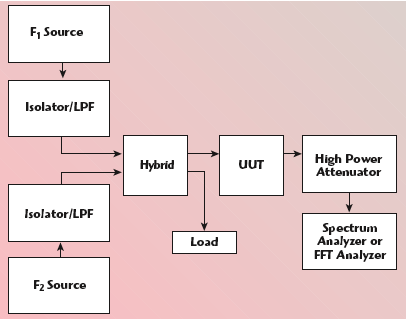
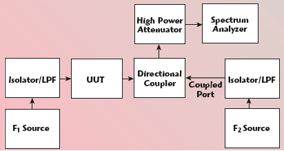
Various schemes1 exist for combining signals from sources F1 and F2 for the two-tone IMD test. Two methods are shown in Figure 1 and 2. In the first method, the two input signals are combined in the forward direction, as in a multi-carrier system. In the second method, the second signal is applied to the output of the ferrite component. This occurs typically in a transmitter combiner or where energy enters a transmitter from a co-located antenna and produces an IMD product. The IMD produced by the second method will generally differ by the isolation of the unit under test (UUT) isolator, from a common feed scheme having identical power levels. Since the two methods often use isolators/circulators in the test bench that are of the same type as those being measured for IMD distortion, some care is required to assure accurate results. Critical considerations are: the isolation between the sources must be sufficient to avoid mixing to occur in the sources. Isolators or circulators other than the UUT must not see full power at both frequencies.
High level mixing must not occur in the spectrum analyzer. The noise floor must be 6 to 10 dB below the IMD level being measured. No spurious response must be visible above the noise floor of the setup when the UUT is replaced by a through connection. If a residual spur is seen that cannot be removed, a sharp filter can be used to reduce the level of F1 or F2, which will reduce the level of the spurious signal. In general, the IMD level is not a strong function of the frequency separation.
The signals F1 and F2 must be kept separate until they enter the UUT so that mixing does not occur external to the UUT. This is accomplished by using a hybrid combiner in the methods discussed here. The disadvantage is that half the input power is lost. However, the hybrid combiner allows arbitrarily small frequency separation and also provides a source match at the IMD frequencies. It is important to maintain source match at IMD frequencies, since the ferrite junction acts more or less as an isotropic source for IMD production, that is, a significant quantity of IMD is emitted from the input port, and if there are sufficient reflections due to a poor source match, it adds vectorially to the IMD emitted from the output port. The result is unequal IMD amplitude levels, even when the input power levels are equal at the two source frequencies. The length of the input cables can also affect the relative IMD amplitudes.
An identified IMD product should be verified by switching off one source at a time, making sure its signal and the IMD signal both disappear on the spectrum analyzer. IMD frequencies must be an integral multiple of the frequency difference between F1 and F2. The spectrum analyzer should be adjusted to have a minimum noise floor 6 to 10 dB below the expected IMD level. When an IMD signal is lost below the noise floor, it may be necessary to slow the sweep, narrow the scan, and/or use averaging. If the sources and the spectrum analyzer are synthesized, synchronizing all three instruments to one of the synthesizer 10 MHz clocks will further lower the noise floor.
Results
Above-resonance drop-in isolators, fed with two +43 dBm common feed carriers, produce third-order IMD between –65 and –95 dBc, depending on the bandwidth, junction size and packaging techniques employed. Production isolators are available with IMDs of –85 dBc over wide temperature ranges for frequencies between 800 and 2200 MHz. Typically these devices are somewhat larger than conventional isolators since they have larger and stronger magnets and bigger circuit geometries. Because of the higher 4πMs and higher fields used at higher frequencies, isolators in the 2200 MHz range have slightly better IMD (a few dB) than those in the 800 MHz range.
References
1. R.D. Billings, “Passive IMD in Ferrites and Filters,” Narda-West Catalog, Application Notes, p. 48
2. K.A. Simons, “The Decibel Relationships Between Amplifier Distortion Products,” Proceedings of the IEEE, July 1970, p. 1071.
3. S.A. Maas, “Volterra Analysis of Spectral Re-growth,” IEEE Microwave and Guided Wave Letters, Vol. 7, No. 7, July 1997, pp. 192–193.
4. H. Bosma, “On Stripline Y-Circulation at UHF,” IEEE Transactions on Microwave Theory and Techniques, Vol. 12, No. 1, January 1964, pp. 61–72.
5. C.E. Fay and R.L. Comstock “Operation of the Ferrite Junction Circulator,” IEEE Transactions on Microwave Theory and Techniques, Vol. 13, No. 1, January 1965, pp. 15–27.
6. Y.S. Wu, W.H. Ku and J.E. Erickson, “A Study of Nonlinearities and Intermodulation Characteristics of 3-Port Distributed Circulators,” IEEE Transactions on Microwave Theory and Techniques, Vol. 24, No. 2, February 1976, pp. 69-77.
7. J.E. Erickson, “Intermodulation Reduction in VHF Communications Systems,” Rome Air Development Center, RADC-TR-75-224, September 1975.
8. H. Suhl, “The Nonlinear Behavior of Ferrites at High Microwave Signal Levels,” Proceedings of the IRE, Vol. 44, 1956, pp. 1270–1283.
9. J.A. Jargon, D.C. DeGroot and K.L. Reed, “NIST Passive Intermodulation Comparison for Wireless Base Station Equipment,” 52nd AFTRG Conference Digest, December 1998, p. 128.
10. Bond, et al., “Intermodulation Generation by Electron Tunneling Through Aluminum-oxide Films,” IEEE Proceedings, December 1979, p. 1643.
11. Arzam, et al., “Nonlinear Metallic Contacts at Microwave Frequency,” IEEE Transactions on Electromagnetic Compatibility, August 1980, p. 142.
Tony Edridge received his BSc degree in electronics from the University of Southampton, England, UK, in 1961, and his doctorate in physics from the University of Surrey, England, UK, in 1973. Before joining M2 Global Technology Ltd. as manager of engineering, he served as vice president of engineering at Sextant Electronics, developing military and aerospace electronic systems. His experience includes management positions in quality, production engineering and software engineering. His early years in industry were spent in R&D of Gunn effect oscillators as senior principal scientist for the Plessey Co. and then creating the first mm-wave cooled receiver for the University of Texas at the McDonald Observatory.